
Datasheet


DTM63368
2 GB - 256Mx72, 240-Pin Unbuffered ECC DDR2 DIMM
Document 06989, Revision A, 06-FEB-08, Dataram Corporation © 2008 Page 9
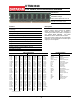
Latency = 4 - X
Latency = 5 - X
Latency = 6 -
TBD -
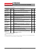
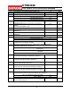
19 DIMM Mechanical Characteristics. Max. module thickness. (mm) x </= 4.10 0x01
20 DIMM type information 0x02
Regular RDIMM (133.35mm) -
Regular UDIMM (133.35mm) - X
SODIMM (67.6mm) -
Micro-DIMM (45.5mm) -
Mini RDIMM (82.0mm) -
Mini UDIMM (82.0mm) -
TBD -
TBD -
21 SDRAM Module Attributes (Refer to Byte20 for DIMM type information). 0x00
Number of active registers on the DIMM (N/A for UDIMM)
-
1
Number of PLL on the DIMM (N/A for UDIMM) - 0
FET Switch External Enable - No
TBD -
Analysis probe installed - No
TBD -
22 SDRAM Device Attributes: General 0x02
Includes Weak Driver -
Supports 50 ohm ODT - X
Supports PASR (Partial Array Self Refresh) -
TBD -
TBD -
TBD -
TBD -
TBD -
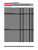
23 Minimum Clock Cycle Time at Reduced CAS Latency, CL
= X-1 (ns)
3.75 0x3D
24 Maximum Data Access Time (tAC ) from Clock at CL = X-
1 (ns)
0.4 0x40
25 Minimum Clock Cycle Time at CL = X-2 (ns) UNUSED 0x00
26 Maximum Data Access Time (tAC ) from Clock at CL = X-
2 (ns)
UNUSED 0x00
27 Minimum Row Precharge Time (tRP ) (ns) 12.5 0x32
28 Minimum Row Active to Row Active Delay (tRRD ) (ns) 7.5 0x1E
29 Minimum RAS to CAS Delay (tRCD ) (ns) 12.5 0x32
30 Minimum Active to Precharge Time (tRAS ) (ns) 45 0x2D
31 Module Rank Density 1GB 0x01
32 Address and Command Setup Time Before Clock (tIS)
(ns)
0.17 0x17
33 Address and Command Hold Time After Clock (tIH) (ns) 0.25 0x25
34 Data Input Setup Time Before Strobe (tDS) (ns) 0.05 0x05
35 Data Input Hold Time After Strobe (tDH) (ns) 0.12 0x12
36 Write Recovery Time (tWR ) (ns) 15 0x3C