
Datasheet


DTM64313H
4GB - 240-Pin 2Rx4 Registered ECC DDR3 DIMM
Document 06606, Revision A, 08-Sep-10, Dataram Corporation © 2010 Page 5
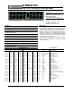
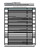
Differential Input Logic Levels (T
A
= 0 to 70 C, Voltage referenced to V
ss
= 0 V)
PARAMETER S
y
mbol Minimum Maximum Unit
Differential Input Logic High
V
IH.DIFF
+0.200 DC:V
DD
AC:V
DD
+0.4 V
Differential Input Logic Low
V
IL.DIFF
DC:V
SS
AC:V
SS
-0.4 -0.200 V
Differential Input Cross Point Voltage
relative to VDD/2
V
IX
- 0.150
+ 0.150 V
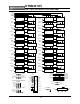
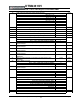
Capacitance (T
A
= 25 C, f = 100 MHz)
PARAMETER Pin Symbol Min. Max. Unit
Input Capacitance, Clock
CK0, /CK0 C
CK
1.5 2.5 pF
Input Capacitance, Address
BA[2:0], A[15:0], /RAS, /CAS, /WE C
I
1.5 2.5 pF
Input Capacitance Control
/S[1:0], CKE[1:0], ODT[1:0] C
I
1.5 2.5 pF
Input/Output Capacitance
DQ[63:0], CB[7:0] DQS[17:0], /DQS[17:0] C
IO
3 5 pF
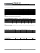
DC Characteristics
(T
A
= 0 to 70 C, Voltage referenced to V
ss
= 0 V)
PARAMETER Symbol Minimum Maximum Unit Note
Input Leakage Current
(Any input 0 V < VIN < VDD)
I
IL
-18 +18 μA 1,2
Output Leakage Current
(0V < VOUT < VDDQ)
I
OL
-10 +10 μA 2,3
Notes:
1) All other pins not under test = 0 V
2) Values are shown per pin
3) DQ, DQS, DQS and ODT are disabled