
Datasheet

DTM64328D
4GB - 240-Pin 2Rx8 Registered ECC DDR3 DIMM
Document
06944
, Revision A, 3-Oct-11, Dataram Corporation
2011 Page 8
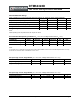
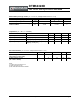
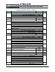
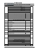
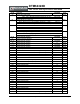
SERIAL PRESENCE DETECT MATRIX
Byte# Function. Value Hex
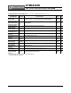
0 Number of Bytes Used / Number of Bytes in SPD Device / CRC Coverage. 0x92
Bit 3 ~ Bit 0. SPD Bytes Used -
176
Bit 6 ~ Bit 4. SPD Bytes Total -
256
Bit 7. CRC Coverage -
Bytes 0-
116
1 SPD Revision. Rev. 1.1
0x11
2 Key Byte / DRAM Device Type. DDR3
SDRAM
0x0B
3 Key Byte / Module Type.
0x01
Bit 3 ~ Bit 0. Module Type -
RDIMM
Bit 7 ~ Bit 4. Reserved -
0
4 SDRAM Density and Banks. 0x02
Bit 3 ~ Bit 0. Total SDRAM capacity, in megabits -
1Gb
Bit 6 ~ Bit 4. Bank Address Bits -
8 banks
Bit 7. Reserved -
0
5 SDRAM Addressing. 0x19
Bit 2 ~ Bit 0. Column Address Bits -
10
Bit 5 ~ Bit 3. Row Address Bits -
15
Bit 7, 6. Reserved
0
6 Reserved. UNUSED 0x00
7 Module Organization. 0x09
Bit 2 ~ Bit 0. SDRAM Device Width -
8-
Bits
Bit 5 ~ Bit 3. Number of Ranks -
2-
Rank
Bit 7, 6. Reserved
0
8 Module Memory Bus Width. 0x0B
Bit 2 ~ Bit 0. Primary bus width, in bits -
64-
Bits
Bit 4, Bit 3. Bus width extension, in bits -
8-B
its
Bit 7 ~ Bit 5. Reserved -
0
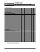
9 Fine Timebase (FTB) Dividend / Divisor. 0x52
Bit 3 ~ Bit 0. Fine Timebase (FTB) Divisor
2
Bit 7 ~ Bit 4. Fine Timebase (FTB) Dividend
5
10 Medium Timebase (MTB) Dividend. 1 (MTB =
0.125ns)
0x01
11 Medium Timebase (MTB) Divisor. 8 (MTB =
0.125ns)
0x08
12 SDRAM Minimum Cycle Time (tCKmin). 1.5ns 0x0C
13 Reserved. UNUSED 0x00
14 CAS Latencies Supported, Least Significant Byte. 0x3C
Bit 0. CL = 4 -
Bit 1. CL = 5 -
Bit 2. CL = 6 -
X
Bit 3. CL = 7 -
X
Bit 4. CL = 8 -
X
Bit 5. CL = 9 -
X
Bit 6. CL = 10 -
Bit 7. CL = 11 -