
Datasheet


DTM64360C
2GB - 240-Pin 1Rx8 Registered ECC DDR3 DIMM
Document 06145, Revision A, 7-Dec-12 Dataram Corporation © 2012 Page 7
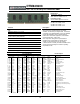
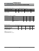
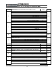
AC Operating Conditions
PARAMETER Symbol Min Max Unit
Internal read command to first data
t
AA
13.125 20 ns
CAS-to-CAS Command Delay
t
CCD
4 - t
CK
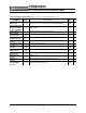
Clock High Level Width
t
CH(avg)
0.47 0.53 t
CK
Clock Cycle Time
t
CK
1.5 1.875 ns
Clock Low Level Width
t
CL(avg)
0.47 0.53 t
CK
Data Input Hold Time after DQS Strobe
t
DH
65 - ps
DQ Input Pulse Width
t
DIPW
400 - ps
DQS Output Access Time from Clock
t
DQSCK
-255 +255 ps
Write DQS High Level Width
t
DQSH
0.45 0.55 t
CK(avg)
Write DQS Low Level Width
t
DQSL
0.45 0.55 t
CK(avg)
DQS-Out Edge to Data-Out Edge Skew
t
DQSQ
- 125 ps
Data Input Setup Time Before DQS Strobe
t
DS
30 - ps
DQS Falling Edge from Clock, Hold Time
t
DSH
0.2
- t
CK(avg)
DQS Falling Edge to Clock, Setup Time
t
DSS
0.2
- t
CK(avg)
Clock Half Period
t
HP
minimum of t
CH
or t
CL
- ns
Address and Command Hold Time after Clock
t
IH
140 - ps
Address and Command Setup Time before Clock
t
IS
65 - ps
Load Mode Command Cycle Time
t
MRD
4 - t
CK
DQ-to-DQS Hold
t
QH
0.38
- t
CK(avg)
Active-to-Precharge Time
t
RAS
36 9*t
REFI
ns
Active-to-Active / Auto Refresh Time
t
RC
49.125 - ns
RAS-to-CAS Delay
t
RCD
13.125 - ns
Average Periodic Refresh Interval 0
o
C < T
CASE
< 85
o
C
t
REFI
- 7.8 μs
Average Periodic Refresh Interval 0
o
C < T
CASE
< 95
o
C
t
REFI
- 3.9 μs
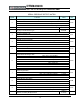
Auto Refresh Row Cycle Time
t
RFC
160 - ns
Row Precharge Time
t
RP
13.125 - ns
Read DQS Preamble Time
t
RPRE
0.9
Note-1
t
CK(avg)
Read DQS Postamble Time
t
RPST
0.3
Note-2
t
CK(avg)
Row Active to Row Active Delay
t
RRD
Max(4nCK, 6ns) - ns
Internal Read to Precharge Command Delay
t
RTP
Max(4nCK, 7.5ns) - ns
Write DQS Preamble Setup Time
t
WPRE
0.9 - t
CK(avg)
Write DQS Postamble Time
t
WPST
0.3 - t
CK(avg)
Write Recovery Time
t
WR
15 - ns
Internal Write to Read Command Delay
t
WTR
Max(4nCK, 7.5ns) - ns
Notes:
1. The maximum preamble is bound by tLZDQS(min)
The maximum postamble is bound by tHZDQS(max)