
Datasheet


DTM64360C
2GB - 240-Pin 1Rx8 Registered ECC DDR3 DIMM
Document 06145, Revision A, 7-Dec-12 Dataram Corporation © 2012 Page 9
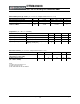
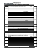
11
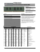
Medium Timebase (MTB) Divisor.
8 (MTB =
0.125ns)
0x08
12
SDRAM Minimum Cycle Time (tCKmin).
1.5ns 0x0C
13 Reserved. UNUSED 0x00
CAS Latencies Supported, Least Significant Byte.
Bit 0. CL = 4 -
Bit 1. CL = 5 -
Bit 2. CL = 6 - X
Bit 3. CL = 7 - X
Bit 4. CL = 8 - X
Bit 5. CL = 9 - X
Bit 6. CL = 10 -
14
Bit 7. CL = 11 -
0x3C
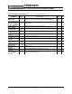
CAS Latencies Supported, Most Significant Byte.
Bit 0. CL = 12 -
Bit 1. CL = 13 -
Bit 2. CL =14 -
Bit 3. CL = 15 -
Bit 4. CL = 16 -
Bit 5. CL = 17 -
Bit 6. CL = 18 -
15
Bit 7. Reserved.
0x00
16 Minimum CAS Latency Time (tAAmin). 13.125ns 0x69
17 Minimum Write Recovery Time (tWRmin). 15.0ns 0x78
18 Minimum RAS# to CAS# Delay Time (tRCDmin). 13.125ns 0x69
19 Minimum Row Active to Row Active Delay Time (tRRDmin). 6.0ns 0x30
20 Minimum Row Precharge Delay Time (tRPmin). 13.125ns 0x69
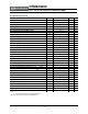
Upper Nibbles for tRAS and tRC.
Bit 3 ~ Bit 0. tRAS Most Significant Nibble - 1
21
Bit 7 ~ Bit 4. tRC Most Significant Nibble - 1
0x11
22
Minimum Active to Precharge Delay Time (tRASmin), Least Significant
Byte.
36.0ns 0x20
23
Minimum Active to Active/Refresh Delay Time (tRCmin), Least
Significant Byte.
49.125ns 0x89
24
Minimum Refresh Recovery Delay Time (tRFCmin), Least Significant
Byte.
160.0ns 0x00
25
Minimum Refresh Recovery Delay Time (tRFCmin), Most Significant
Byte.
160.0ns 0x05
26 Minimum Internal Write to Read Command Delay Time (tWTRmin). 7.5ns 0x3C
27 Minimum Internal Read to Precharge Command Delay Time (tRTPmin). 7.5ns 0x3C
Upper Nibble for tFAW.
Bit 3 ~ Bit 0. tFAW Most Significant Nibble - 0
28
Bit 7 ~ Bit 4. Reserved - 0
0x00