
Datasheet

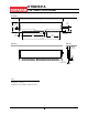


DTM65521A
2 GB - 256Mx72, 240-Pin FB-DIMM
Document 06054, Revision A, 1-Aug-08, Dataram Corporation © 2008 Page 4
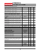
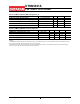
Absolute Maximum Ratings
Parameter Symbol Rating Unit Note
Temperature, DDR2 DRAM Case
T
Case
0 to +95 C 1, 2
Temperature, Storage
T
STG
-55 to +100 C 1
Voltage on any pin relative to V
SS
V
IN
,V
OUT
-0.3 to 1.75 V 1
Voltage on V
CC
relative to V
SS
V
CC
-0.3 to 1.75 V 1
Voltage on V
DD
relative to V
SS
V
DD
-0.5 to 2.3 V 1
Voltage on V
TT
relative to V
SS
V
TT
-0.5 to 2.3 V 1
Power Dissipation
P
D
21 W 1
NOTES:
1. Operation at or above absolute maximum rating can adversely affect device reliability.
2. For 85 C < T
Case
≤ 95 C, t
REFI
= 3.9 μs max.
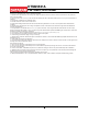
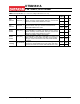
DC Operating Conditions (T
A
= 0 to 70 C, Voltage referenced to V
SS
= 0V)
Parameter Symbol Minimum Typical Maximum Unit Note
AMB Supply Voltage
V
CC
1.425 1.5 1.59 V
DDR2 Supply Voltage
V
DD
1.7 1.8 1.9 V
Termination Voltage
V
TT
0.48 x V
DD 0.50 x VDD 0.52 x VDD
V
EEPROM Supply Voltage (SPD)
V
DDSPD
3.0 3.3 3.6 V
Input High Voltage (SPD)
V
IH(DC)
2.1 V
DDSPD
V 1
Input Low Voltage (SPD)
V
IL(DC)
1.0 V 1
Input High Voltage (RESET/BFUNC)
V
IH(DC)
1.0 V 2
Input Low Voltage( RESET/BFUNC)
V
IL(DC)
0.5 V 1
Leakage Curent (RESET/BFUNC)
I
L
-90 90 μA 2
Leakage Curent (Link)
I
L
-5 5 μA
Notes:
1. Applies to SMB and SPD bus signals.
2. Applies to AMB CMOS signal /RESET.