
Datasheet


DTM67220
1GB 200-Pin 1Rx8 Unbuffered Non-ECC DDR2 SO-DIMM
Document 06833, Revision A, 28-Sep-11, Dataram Corporation
2011 Page 5
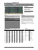
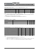
Differential Input Logic Levels (T
A
= 0 to 70 C, Voltage referenced to V
ss
= 0 V)
PARAMETER
Symbol
Minimum
Maximum
Unit
Note
DC Input Signal Voltage
V
IN(DC)
-0.300 V
DD
+ 0.300 V 1
DC Differential Input Voltage
V
ID(DC)
-0.250 V
DD
+ 0.600 V 2
AC Differential Input Voltage
V
ID(AC)
-0.500 V
DD
+ 0.600 V 3
AC Differential Cross-Point Voltage
V
IX(AC)
0.50 V
DD
- 0.175
0.50 V
DD
+ 0.175 V 4
Notes:
1. V
IN(DC)
specifies the allowable DC excursion of each input of a differential pair.
2. V
ID(DC)
specifies the input differential voltage, i.e. the absolute value of the difference between the two voltages of a differential
pair.
3. V
ID(AC)
specifies the input differential voltage required for switching.
4. The typical value of V
IX(AC)
is expected to be 0.5 V
DD
and is expected to track variations in V
DD
.
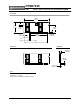
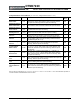
Capacitance (T
A
= 25 C, f = 100 MHz)
PARAMETER Pin
Symbol Min. Max. Unit
Input Capacitance, Clock
CK[1:0], /CK[1:0] CIN1 4 8 pF
Input Capacitance, Address
and Control
BA[2:0], A[13:0], /RAS, /CAS, /WE, ODT0, CKE0, /S0 CIN2 8 14 pF
Input/Output Capacitance
DQ[63:0], DQS[7:0], /DQS[7:0], DM[7:0] CIO 2.5 3.5 pF
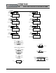
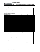
DC Characteristics
(T
A
= 0 to 70 C, Voltage referenced to V
ss
= 0 V)
PARAMETER Symbol Minimum Maximum Unit Note
Input Leakage Current Command and Address
I
LI
-80 80 µA 1
Input Leakage Current /S0, CKE0, ODT0
I
LI
-40 40 µA 1
Input Leakage Current CK[1:0], /CK[1:0]
I
LI
-30 30 µA 1
Input Leakage Current DM
I
LI
-10 10 µA 1
Output Leakage Current DQS, DQ
I
OZ
-10 10 µA 2
Output Minimum Source DC Current
I
OH
-13.4 - mA 3
Output Minimum Sink DC Current
I
OL
+13.4 - mA 4
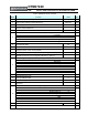
Notes:
1. These values are guaranteed by design and are tested on a sample basis only
2. DQx and ODT are disabled, and 0 V ≤ V
OUT
≤ V
DD
.
3. V
DD
= 1.7 V, V
OUT
= 1420 mV. (V
OUT
- V
DD
)/I
OH
must be less than 21 Ohms for values of V
OUT
between V
DD
and (V
DD
- 280
mV).
4. V
DD
= 1.7 V, V
OUT
= 280 mV. V
OUT
/I
OL
must be less than 21 Ohms for values of V
OUT
between 0 V and 280 mV.