
Datasheet
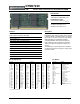
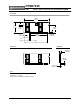
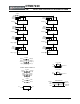


DTM67220
1GB 200-Pin 1Rx8 Unbuffered Non-ECC DDR2 SO-DIMM
Document 06833, Revision A, 28-Sep-11, Dataram Corporation
2011 Page 6
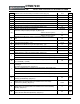
I
DD
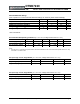
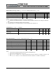
Specifications and Conditions
(T
A
= 0 to 70 C, Voltage referenced to V
ss
= 0 V)
PARAMETER Symbol Test Condition
Max
Value
Unit
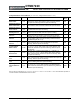
Operating One
Bank Active-
Precharge Current
I
DD
0
CKE is HIGH, /CS is HIGH between valid commands; Address
bus inputs are switching; Data bus inputs are switching.
360 mA
Operating One
Bank Active-Read-
Precharge Current
I
DD
1
I
OUT
= 0 mA; BL = 4, CL = 5 ns, AL = 0; CKE is HIGH, /CS is
HIGH between valid commands; Address bus inputs are switch-
ing.
408 mA
Precharge Power-
Down Current
I
DD
2P
All banks idle; CKE is LOW; Other control and address bus inputs
are stable; Data bus inputs are floating.
80 mA
Precharge Quiet
Standby Current
I
DD
2Q
All banks idle; CKE is HIGH, /CS is HIGH; Other control and ad-
dress bus inputs are stable; Data bus inputs are floating.
160 mA
Precharge Standby
Current
I
DD
2N
All banks idle; CKE is HIGH, /CS is HIGH; Other control and ad-
dress bus inputs are switching; Data bus inputs are switching.
200 mA
Active Power-Down
Current
I
DD
3P
All banks open; CKE is LOW; Other control and address bus in-
puts are stable; Data bus inputs are floating. Fast Power-down
exit (Mode Register bit 12 = 0)
184 mA
Active Standby
Current
I
DD
3N
All banks open; t
RAS
= 70 ms; CKE is HIGH, /CS is HIGH between
valid commands; Other control and address bus inputs are
switching; Data bus inputs are switching.
296 mA
Operating Burst
Write Current
I
DD
4W
All banks open, Continuous burst writes; BL = 4, CL = 5 t
CK
,
AL = 0; t
RAS
= 70 ms, CKE is HIGH, /CS is HIGH between valid
commands; Address bus inputs are switching; Data bus inputs
are switching.
576 mA
Operating Burst
Read Current
I
DD
4R
All banks open, Continuous burst reads, I
OUT
= 0 mA; BL = 4,
CL = 5 t
CK
, AL = 0, t
RAS
= 70 ms; CKE is HIGH, /CS is HIGH be-
tween valid commands; Address bus inputs are switching; Data
bus inputs are switching.
640 mA
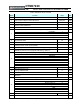
Burst Refresh Cur-
rent
I
DD
5
Refresh command at every 75 ns; CKE is HIGH, /CS is HIGH be-
tween valid commands; Other control and address bus inputs are
switching; Data bus inputs are switching.
840 mA
Self Refresh Cur-
rent
I
DD
6
CK and /CK at 0 V; CKE ≤ 0.2 V; Other control and address bus
inputs are floating; Data bus inputs are floating.
80 mA
Operating Bank In-
terleave Read Cur-
rent
I
DD
7
All bank interleaving reads, I
OUT
= 0 mA; BL = 4, CL = 5 t
CK
;
AL = 70 ns; t
RRD
= 7.5 ns; CKE is HIGH, /CS is HIGH between
valid commands; Address bus inputs are stable during deselects;
Data bus inputs are switching.
1280 mA
Note: For all I
DD
X measurements, t
CK
= 2.5 ns, t
RC
= 60 ns, t
RCD
= 15 ns, t
RAS
= 45 ns, and t
RP
= 15 ns unless otherwise specified. All
currents are based on DRAM absolute maximum values.