
Datasheet


DTM67220
1GB 200-Pin 1Rx8 Unbuffered Non-ECC DDR2 SO-DIMM
Document 06833, Revision A, 28-Sep-11, Dataram Corporation
2011 Page 7
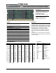
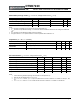
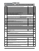
AC Operating Conditions
PARAMETER Symbol Min Max Unit
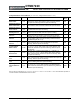
DQ Output Access Time from Clock
t
AC
-400 +400 ps
CAS-to-CAS Command Delay
t
CCD
2 - t
CK
Clock High Level Width
t
CH
0.48 0.52 t
CK
Clock Cycle Time
t
CK
2500 8000 ps
Clock Low Level Width
t
CL
0.48 0.52 t
CK
Data Input Hold Time after DQS Strobe
t
DH
125 - ps
DQ Input Pulse Width
t
DIPW
0.35 - t
CK
DQS Output Access Time from Clock
t
DQSCK
-350 +350 ps
Write DQS High Level Width
t
DQSH
0.35 - t
CK
Write DQS Low Level Width
t
DQSL
0.35 - t
CK
DQS-Out Edge to Data-Out Edge Skew
t
DQSQ
- 200 ps
Data Input Setup Time Before DQS Strobe
t
DS
50 - ps
DQS Falling Edge from Clock, Hold Time
t
DSH
0.2
- t
CK
DQS Falling Edge to Clock, Setup Time
t
DSS
0.2
- t
CK
Clock Half Period
t
HP
minimum of t
CH
or t
CL
- ns
Address and Command Hold Time after Clock
t
IH
250 - ps
Address and Command Setup Time before Clock
t
IS
175 - ps
Load Mode Command Cycle Time
t
MRD
2 - t
CK
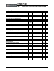
DQ-to-DQS Hold
t
QH
t
HP
- t
QHS
- -
Data Hold Skew Factor
t
QHS
- 400 ps
Active-to-Precharge Time
t
RAS
45 70K ns
Active-to-Active / Auto Refresh Time
t
RC
60 - ns
RAS-to-CAS Delay
t
RCD
15 - ns
Average Periodic Refresh Interval
t
REFI
- 7.8 µs
Auto Refresh Row Cycle Time
t
RFC
127.5 - ns
Row Precharge Time
t
RP
15 - ns
Read DQS Preamble Time
t
RPRE
0.9 1.1 t
CK
Read DQS Postamble Time
t
RPST
0.4 0.6 t
CK
Row Active to Row Active Delay
t
RRD
7.5 - ns
Internal Read to Precharge Command Delay
t
RTP
7.5 - ns
Write DQS Preamble Time
t
WPRE
0.35 - t
CK
Write DQS Postamble Time
t
WPST
0.4 0.6 t
CK
Write Recovery Time
t
WR
15 - ns
Internal Write to Read Command Delay
t
WTR
7.5 - ns
Exit Self Refresh to Non-Read Command
t
XSNR
t
RFC
(min) + 10 - ns
Exit Self Refresh to Read Command
t
XSRD
200 - t
CK