
Datasheet


DTM67220
1GB 200-Pin 1Rx8 Unbuffered Non-ECC DDR2 SO-DIMM
Document 06833, Revision A, 28-Sep-11, Dataram Corporation
2011 Page 9
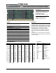
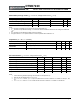
TBD -
TBD -
Latency = 2 -
Latency = 3 -
Latency = 4 -
X
Latency = 5 -
X
Latency = 6 -
X
TBD -
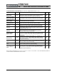
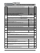
19 DIMM Mechanical Characteristics. Max. module thickness. (mm) x </= 3.80 0x01
DIMM type information 0x04
Regular RDIMM (133.35mm) -
Regular UDIMM (133.35mm) -
SODIMM (67.6mm) -
X
Micro-DIMM (45.5mm) -
Mini RDIMM (82.0mm) -
Mini UDIMM (82.0mm) -
TBD -
20
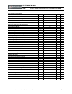
TBD -
SDRAM Module Attributes (Refer to Byte20 for DIMM type information). 0x00
Number of active registers on the DIMM (N/A for UDIMM) -
1
Number of PLL on the DIMM (N/A for UDIMM) -
0
FET Switch External Enable -
No
TBD -
Analysis probe installed -
No
21
TBD -
SDRAM Device Attributes: General 0x03
Includes Weak Driver -
X
Supports 50 ohm ODT -
X
Supports PASR (Partial Array Self Refresh) -
TBD -
TBD -
TBD -
TBD -
22
TBD -
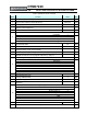
23 Minimum Clock Cycle Time at Reduced CAS Latency, CL = X-1 (ns) 3 0x30
24 Maximum Data Access Time (tAC ) from Clock at CL = X- 1 (ns) 0.4 0x40
25 Minimum Clock Cycle Time at CL = X-2 (ns) 3.75 0x3D
26 Maximum Data Access Time (tAC ) from Clock at CL = X-2 (ns) 0.4 0x40
27 Minimum Row Precharge Time (tRP ) (ns) 15 0x3C
28 Minimum Row Active to Row Active Delay (tRRD ) (ns) 7.5 0x1E
29 Minimum RAS to CAS Delay (tRCD ) (ns) 15 0x3C
30 Minimum Active to Precharge Time (tRAS ) (ns) 45 0x2D
31 Module Rank Density
1GB
0x01