
Datasheet


DTM68103B
4GB - 288-Pin 1Rx8 Unbuffered Non- ECC DDR4 DIMM
Document 06386, Revision A, 08-Sep-14, Dataram Corporation © 2014 Page 3
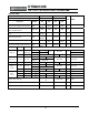
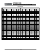
Speed Bin Table Notes:
Absolute Specification
- VDDQ = VDD = 1.20V +/- 0.06 V
- VPP = 2.5V +0.25/-0.125 V
- The values defined with above-mentioned table are DLL ON case.
- DDR4-1600, 1866, 2133 and 2400 Speed Bin Tables are valid only when Geardown Mode is disabled.
1. The CL setting and CWL setting result in tCK(avg).MIN and tCK(avg).MAX requirements. When making a selection of tCK(avg),
both need to be fulfilled: Requirements from CL setting as well as requirements from CWL setting.
2. tCK(avg).MIN limits: Since CAS Latency is not purely analog - data and strobe output are synchronized by the DLL – all possible
intermediate frequencies may not be guaranteed. An application should use the next smaller JEDEC standard tCK(avg) value
(1.5, 1.25, 1.071, 0.938 or 0.833 ns) when calculating CL [nCK] = tAA [ns] / tCK(avg) [ns], rounding up to the next ‘Supported CL’,
where tAA = 12.5ns and tCK(avg) = 1.3 ns should only be used for CL = 10 calculation.
3. tCK(avg).MAX limits: Calculate tCK(avg) = tAA.MAX / CL SELECTED and round the resulting tCK(avg) down to the next valid
speed bin (i.e. 1.5ns or 1.25ns or 1.071 ns or 0.938 ns or 0.833 ns). This result is tCK(avg). MAX corresponding to CL
SELECTED.
4. ‘Reserved’ settings are not allowed. User must program a different value.
5. 'Optional' settings allow certain devices in the industry to support this setting however it is not a mandatory feature. Refer to
supplier's data sheet and/or the DIMM SPD information if and how this setting is supported.
6. Any DDR4-2133 speed bin also supports functional operation at lower frequencies as shown in the table which are not subject to
Production Tests but verified by Design/Characterization.
7. DDR4-1600 AC timing apply if DRAM operates at lower than 1600 MT/s data rate.
8. For devices supporting optional down binning to CL=9, CL=11 and CL=13, tAA/tRCD/tRPmin must be 13.5ns or lower. SPD
settings must be programmed to match. For example, DDR4-1600K devices supporting down binning to 1333MT/s should
program 13.5ns in SPD bytes for tAAmin(Byte 24), tRCDmin (Byte 25), and tRPmin (Byte 26). DDR4-1866M devices supporting
down binning to 1333MT/s or DDR4-1600K should program 13.5ns in SPD bytes for tAAmin (Byte 24), tRCDmin (Byte 25), and
tRPmin (Byte 26).DDR4-2133P devices supporting down binning to 1333MT/s or DDR4-1600K or DDR4-1866M should program
13.5ns in SPD bytes for tAAmin (Byte 24), tRCDmin (Byte 25), and tRPmin (Byte 26).tRCmin (Byte 27, 29) also should be
programmed accordingly. For example, 48.5ns (tRASmin + tRPmin = 35ns+ 13.5ns) is set to supporting optional down binning
CL=9 and CL=11.
9. CL number in parentheses, it means that these numbers are optional.
10. DDR4 SDRAM supports CL=9 as long as a system meets tAA(min).