
Datasheet


DTM68103B
4GB - 288-Pin 1Rx8 Unbuffered Non- ECC DDR4 DIMM
Document 06386, Revision A, 08-Sep-14, Dataram Corporation © 2014 Page 5
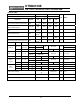
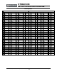
PINDESCRIPTION
Name Function
CB[7:0] * Data Check Bits
DQ[63:0] Data Bits
DM[7:0]_n, DBI[7:0]_n Input Data Mask and Data Bus Inversion
DQS[7:0]_t, DQS[7:0]_c Differential Data Strobes
CK_t[1:0], CK_c[1:0] Differential Clock Inputs
CKE0, CKE1* Clock Enables
CAS_n / A15 Multiplexed: Column Address Strobe or Address 15
RAS_n / A16 Multiplexed: Row Address Strobe or Address 16
CS0_N,CS[3:1]_n* Chip Selects
ACT_n Activate Command Input
WE_n / A14 Multiplexed: Write Enable or Address 14
C[2:0]* Chip ID Inputs
A[17:0] Address Inputs
BA[1:0] Bank Address select Inputs
BG[1:0] Bank Group select Inputs
ODT0, ODT1* On Die Termination Inputs
SA[2:0] SPD Address
SCL SPD Clock Input
SDA SPD Data Input/Output
EVENT_n Temperature Sensing
RESET_n Reset for register and DRAMs
PARITY Parity bit input for Addr/Ctrl
ALERT_n CRC Error Flag or CMD/Addr Parity Flag Output
A12 / BC_n Combination Input: Address12/Burst Chop
A10 / AP Combination Input: Addr10/Auto-precharge
12V* Optional Power Supply*
V
PP
Charge Pump Power
V
SS
Ground
V
DD
Power
V
DDSPD
SPD EEPROM Power
V
REFCA
Reference Voltage for CA
V
TT
Termination Voltage
NC No Connection
RFU Reserved for Future Use
* Not used