
Datasheet
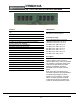


DTM68104A
8GB - 288-Pin 2Rx8 Unbuffered Non-ECC DDR4 DIMM
Document 06416, Revision A, 25-Nov-14, Dataram Corporation © 2014 Page 3
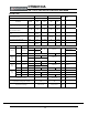
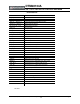
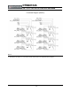
SpeedBinTableNotes:
AbsoluteSpecification
‐VDDQ=VDD=1.20V+/‐0.06V
‐VPP=2.5V+0.25/‐0.125V
‐Thevaluesdefinedwithabove‐mentionedtableareDLLONcase.
‐DDR4‐1600,1866,2133and2400SpeedBinTablesarevalidonlywhenGeardownModeisdisabled.
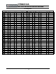
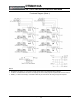
1. The CL setting and CWL setting result in tCK(avg).MIN and tCK(avg).MAX requirements. When making a selection of tCK(avg),
both need to be fulfilled: Requirements from CL setting as well as requirements from CWL setting.
2. tCK(avg).MIN limits: Since CAS Latency is not purely analog - data and strobe output are synchronized by the DLL – all
possible intermediate frequencies may not be guaranteed. An application should use the next smaller JEDEC standard
tCK(avg) value (1.5, 1.25, 1.071, 0.938 or 0.833 ns) when calculating CL [nCK] = tAA [ns] / tCK(avg) [ns], rounding up to
the next ‘Supported CL’, where tAA = 12.5ns and tCK(avg) = 1.3 ns should only be used for CL = 10 calculation.
3. tCK(avg).MAX limits: Calculate tCK(avg) = tAA.MAX / CL SELECTED and round the resulting tCK(avg) down to the next valid
speed bin (i.e. 1.5ns or 1.25ns or 1.071 ns or 0.938 ns or 0.833 ns). This result is tCK(avg). MAX corresponding to CL SELECTED.
4.‘Reserved’settingsarenotallowed.Usermustprogramadifferentvalue.
5.'Optional'settingsallowcertaindevicesintheindustrytosupportthissettinghoweveritisnotamandatoryfeature.
Refertosupplier'sdatasheetand/ortheDIMMSPDinformationifandhowthissettingissupported.
6.Any
DDR4‐1866speedbinalsosupportsfunctionaloperationatlowerfrequenciesasshowninthetablewhicharenot
subjecttoProductionTestsbutverifiedbyDesign/Characterization.
7.AnyDDR4‐2133speedbinalsosupportsfunctionaloperationatlowerfrequenciesasshowninthetablewhicharenot
subjectto
ProductionTestsbutverifiedbyDesign/Characterizatio n.
8.AnyDDR4‐2400speedbinalsosupportsfunctionaloperationatlowerfrequenciesasshowninthetablewhicharenot
subjecttoProductionTestsbutverifiedbyDesign/Characterization.
9.ReservedforDDR4‐2666speedbin.
10.ReservedforDDR4‐3200speedbin.
11.DDR4
‐1600ACtimingapplyifDRAMoperatesatlowerthan1600MT/sdatarate.
12.FordevicessupportingoptionaldownbinningtoCL=9,CL=11andCL=13,tAA/tRCD/tRPminmustbe13.5nsorlower.
SPDsettingsmustbeprogrammedtomatch.Forexample,DDR4‐1600Kdevicessupportingdownbinningto1333MT/s
should
program13.5nsinSPDbytesfortAAmin(Byte24),tRCDmin(Byte25),andtRPmin(Byte26).DDR4‐1866Mdevices
supportingdownbinningto1333MT/sorDDR4‐1600Kshouldprogram13.5nsinSPDbytesfortAAmin(Byte24), tRCDmin
(Byte25),andtRPmin(Byte26).DDR4‐2133Pdevicessupportingdownbinningto1333MT/sor
DDR4‐1600KorDDR4‐1866Mshouldprogram13.5nsinSPDbytesfortAAmin(Byte24),tRCDmin(Byte25),andtRPmin
(Byte26).tRCmin(Byte27,29)alsoshouldbeprogrammedaccordingly.Forexample,48.5ns(tRASmin+tRPmin=35ns+
13.5ns)issettosupportingoptionaldownbinningCL=9andCL=11.
13.
CLnumberinparentheses,itmeansthatthesenumbersareoptional.
14.DDR4SDRAMsupportsCL=9aslongasasystemmeetstAA(min).