
White Papers

Ready Solutions Engineering Test Results
Copyright © 2017 Dell Inc. or its subsidiaries. All Rights Reserved. Dell, EMC, and other trademarks are trademarks of Dell Inc. or its subsidiaries. Other trademarks may be
the property of their respective owners. Published in the USA. Dell EMC believes the information in this document is accurate as of its publication date. The information is
subject to change without notice.
1
Deep Learning on V100
Authors: Rengan Xu, Frank Han, Nishanth Dandapanthula.
HPC Innovation Lab. September 2017
Overview
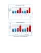
In this blog, we will introduce the NVIDIA Tesla Volta-based V100 GPU and evaluate it with different deep learning frameworks. We will
compare the performance of the V100 and P100 GPUs. We will also evaluate two types of V100: V100-PCIe and V100-SXM2. The results
indicate that in training V100 is ~40% faster than P100 with FP32 and >100% faster than P100 with FP16, and in inference V100 is 3.7x
faster than P100. This is one blog of our Tesla V100 blog series. Another blog of this series is about the general HPC applications
performance on V100 and you can read it here.
Introduction to V100 GPU
In the 2017 GPU Technology Conference (GTC), NVIDIA announced the Volta-based V100 GPU. Similar to P100, there are also two
types of V100: V100-PCIe and V100-SXM2. V100-PCIe GPUs are inter-connected by PCIe buses and the bi-directional bandwidth is up
to 32 GB/s. V100-SXM2 GPUs are inter-connected by NVLink and each GPU has six links and the bi-directional bandwidth of each link
is 50 GB/s, so the bi-directional bandwidth between different GPUs is up to 300 GB/s. A new type of core added in V100 is called tensor
core which was designed specifically for deep learning. These cores are essentially a collection of ALUs for performing 4x4 matrix
operations: specifically a fused multiply add (A*B+C), multiplying two 4x4 FP16 matrices together, and then adding to a FP16/FP32 4x4
matrix to generate a final 4x4 FP16/FP32 matrix. By fusing matrix multiplication and add in one unit, the GPU can achieve high FLOPS
for this operation. A single Tensor Core performs the equivalent of 64 FMA operations per clock (for 128 FLOPS total), and with 8 such
cores per Streaming Multiprocessor (SM), 1024 FLOPS per clock per SM. By comparison, even with pure FP16 operations, the standard
CUDA cores in a SM only generate 256 FLOPS per clock. So in scenarios where these cores can be used, V100 is able to deliver 4x the
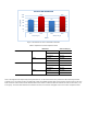
performance versus P100. The detailed comparison between V100 and P100 is in Table 1.
Table 1: The comparison between V100 and P100
P100-PCIe
V100-PCIe
Improvement
P100-SXM2
V100-SXM2
Improvement
CUDA Cores
3584
5120
3584
5120
Tensor Cores
N/A
640
N/A
640
Boost Clock
1329 MHz
1380 MHz
1481 MHz
1530 MHz
Memory Bandwidth
732 GB/s
900 GB/s
22.95%
732 GB/s
900 GB/s
22.95%
NVLink Bi-bandwidth
N/A
N/A
160 GB/s
300 GB/s
Double Precision
4.7 TFLOPS
7 TFLOPS
1.5x
5.3 TFLOPS
7.8 TFLOPS
1.5x
Single Precision
9.3 TFLOPS
14 TFLOPS
1.5x
10.6 TFLOPS
15.7 TFLOPS
1.5x
Deep Learning
18.6 TFLOPS
112 TFLOPS
6x
21.2 TFLOPS
125 TFLOPS
6x
Architecture
Pascal
Volta
Pascal
Volta
TDP
250W
250W
300W
300W
Testing Methodology