locate, communicate, accelerate LEON-G100/G200 quad-band GSM/GPRS Data and Voice Modules System Integration Manual Abstract This document describes the features and integration of the LEON-G100/G200 quad-band GSM/GPRS data and voice modules. The LEON-G100/G200 are complete and cost efficient solutions, bringing full feature quad-band GSM/GPRS data and voice transmission technology in a compact form factor. www.u-blox.com 29.5 x 18.9 x 3.
LEON-G100/G200 - System Integration Manual Document Information Title LEON-G100/G200 Subtitle quad-band GSM/GPRS Data and Voice Modules Document type System Integration Manual Document number GSM.G1-HW-09002-F3 Document status Preliminary Document status information Objective This document contains target values. Revised and supplementary data will be published Specification later. Advance This document contains data based on early testing.
LEON-G100/G200 - System Integration Manual Preface u-blox Technical Documentation As part of our commitment to customer support, u-blox maintains an extensive volume of technical documentation for our products. In addition to our product-specific technical data sheets, the following manuals are available to assist u-blox customers in product design and development.
LEON-G100/G200 - System Integration Manual Contents Preface ................................................................................................................................ 3 Contents.............................................................................................................................. 4 1 System description ....................................................................................................... 7 1.1 1.2 Overview .....................................
LEON-G100/G200 - System Integration Manual 2.1.3 Antenna checklist ........................................................................................................................ 72 2.2 Design Guidelines for Layout .............................................................................................................. 72 2.2.1 Layout guidelines per pin function ............................................................................................... 72 2.2.2 2.2.
LEON-G100/G200 - System Integration Manual B A.6 A.7 HTTP ................................................................................................................................................... 96 SMTP .................................................................................................................................................. 96 A.8 GPS .......................................................................................................................................
LEON-G100/G200 - System Integration Manual 1 System description 1.1 Overview LEON-G100/G200 GSM/GPRS modules integrate a full-featured Release 99 GSM-GPRS protocol stack, with the following main characteristics.
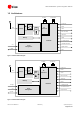
LEON-G100/G200 - System Integration Manual 1.2 Architecture 32.768 kHz 26 MHz Power-On PA ANT Reset SAW Filter Switch RF Transceiver GPIO DDC (for GPS) SIM Card Memory UART Baseband 2 Analog Audio Headset Detection Vcc Power Management Digital Audio V_BCKP ADC Figure 1: LEON-G100 block diagram 32.
LEON-G100/G200 - System Integration Manual 1.2.1 Functional blocks LEON-G100/G200 modules consist of the following functional blocks: RF Baseband Power Management 1.2.1.1 RF The RF block is composed of the following main elements: RF transceiver (integrated in the GSM/GPRS single chip) performing modulation, up-conversion of the baseband I/Q signals, down-conversion and demodulation of the RF received signals.
LEON-G100/G200 - System Integration Manual 1.3 Pin-out Table 1 describes the pin-out of LEON-G100/G200 modules, with pins grouped by function. Function Pin No I/O Description Remarks Power VCC 50 I Module Supply GND 1, 3, 6, 7, 8, 17, 25, 36, 45, 46, 48, 49 N/A Ground Clean and stable supply is required: low ripple and low voltage drop must be guaranteed. Voltage provided has to be always above the minimum limit of the operating range.
LEON-G100/G200 - System Integration Manual Function Pin No I/O Description Remarks SPK_N 39 O MIC_BIAS2 41 I MIC_GND2 42 I MIC_GND1 43 I MIC_BIAS1 44 I SIM_CLK 32 O Second speaker output with power differential analog audio output Second microphone analog signal input and bias output Second microphone analog reference First microphone analog reference First microphone analog signal input and bias output SIM clock SIM_IO 33 I/O SIM data This audio output is used when audio downl
LEON-G100/G200 - System Integration Manual 1.4 Operating modes LEON-G100/G200 modules include several operating modes, each have different features and interfaces. Table 2 summarizes the various operating modes and provides general guidelines for operation. Operating Mode Description Features / Remarks Transition condition Module is switched off. Application interfaces are not accessible. Internal RTC timer operates only if a valid voltage is applied to V_BCKP pin.
LEON-G100/G200 - System Integration Manual Operating Mode Description Features / Remarks Connected-Mode Voice or data call enabled. Microprocessor runs with 26 MHz as reference oscillator. Module is ready to accept data signals from an external device. The module is switched on and a voice call or a data call (GSM/GPRS) is in progress. Module is fully active. Application interfaces are enabled. When call terminates, module returns to the last operating state (Idle or Active).
LEON-G100/G200 - System Integration Manual 1.5 Power management 1.5.1 Power supply circuit overview LEON-G100/G200 4-Bands GSM FEM Antenna Switch PA GSM/GPRS Chipset Charging Control VCC LDOs RF LDOs BB LDO EBU 50 2 x 22 µF MCP Memory NOR Flash LDO PSRAM LDO V_BCKP RTC 2 1 µF VSIM 35 1 µF Figure 3: Power supply concept Power supply is via VCC pin. This is the only one main power supply pin.
LEON-G100/G200 - System Integration Manual 1.5.2 Module supply (VCC) LEON-G100/G200 modules must be supplied through VCC pin by a DC power supply. Voltages must be stable, due to the surging consumption profile of the GSM system (described in the section 1.5.3). Name Description Remarks VCC Module Supply GND Ground Clean and stable supply is required: low ripple and low voltage drop must be guaranteed. Voltage provided has to be always above the minimum limit of the operating range.
LEON-G100/G200 - System Integration Manual o o Voltage drop during transmit slots has to be lower than 400 mV Undershoot and overshoot at the start and at the end of transmit slots have to be not present o Voltage ripple during transmit slots has to be: lower than 100 mVpp if fripple ≤ 200 kHz lower than 10 mVpp if 200 kHz < fripple ≤ 400 kHz lower than 2 mVpp if fripple > 400 kHz Voltage overshoot ripple 3.
LEON-G100/G200 - System Integration Manual Main Supply Available? No, portable device Battery Li-Ion 3.7 V Yes, always available Main Supply Voltage >5 V? No, less than 5 V Linear LDO Regulator Yes, greater than 5 V Switching Step-Down Regulator Figure 5: VCC supply concept selection The switching step-down regulator is the typical choice when the available primary supply source has a nominal voltage much higher (e.g. greater than 5 V) than the LEON-G100/G200 operating supply voltage.
LEON-G100/G200 - System Integration Manual PWM mode and high efficiency burst or PFM mode can be used, provided the mode transition occurs when the GSM module changes status from idle mode (current consumption approximately 1 mA) to active mode (current consumption approximately 100 mA): it is permissible to use a regulator that switches from the PWM mode to the burst or PFM mode at an appropriate current threshold (e.g.
LEON-G100/G200 - System Integration Manual 12V LEON-G100 LEON-G200 8 VCC OUT 1 3 INH D1 C1 6 FSW C6 R5 U1 2 SYNC R1 R3 C3 FB 5 COMP 4 50 VCC L1 C4 R4 C2 R2 GND 7 GND C5 Figure 7: Suggested schematic design for the VCC voltage supply application circuit using a low cost step-down regulator Reference Description Part Number - Manufacturer C1 C2 22 µF Capacitor Ceramic X5R 1210 10% 25 V 100 µF Capacitor Tantalum B_SIZE 20% 6.
LEON-G100/G200 - System Integration Manual LEON-G100 LEON-G200 5V 2 IN OUT 4 50 VCC U1 C1 R1 R2 1 SHDN ADJ GND 3 C2 5 GND R3 Figure 8: Suggested schematic design for the VCC voltage supply application circuit using an LDO linear regulator Reference Description Part Number - Manufacturer C1 10 µF Capacitor Ceramic X5R 0603 20% 6.3 V GRM188R60J106ME47 - Murata C2 10 µF Capacitor Ceramic X5R 0603 20% 6.3 V GRM188R60J106ME47 - Murata R1 R2 47 kΩ Resistor 0402 5% 0.1 W 4.
LEON-G100/G200 - System Integration Manual Maximum pulse and DC discharge current: the no-rechargeable battery with its output circuit has to be capable to deliver 2.5 A current pulses with 1/8 duty cycle to VCC pin and has to be capable to deliver a DC current greater than the module maximum average current consumption to VCC pin.
LEON-G100/G200 - System Integration Manual 1.5.3 Current consumption profiles During operation, the current consumed by LEON-G100/G200 through VCC pin can vary by several orders of magnitude. This is applied to ranges from the high peak of current consumption during the GSM transmitting bursts at maximum power level in connected mode, to the low current consumption in idle mode when power saving configuration is enabled. 1.5.3.
LEON-G100/G200 - System Integration Manual In the following figure is reported the current consumption profiles with 2 slots used to transmit. Current [A] 2.5 2.0 1800 mA 1.5 Peak current depends on TX power 1.0 0.5 ~170 mA 0.0 RX slot 200mA ~170 mA ~40 mA unused unused slot slot TX slot TX slot unused slot MON slot unused slot RX slot unused unused slot slot GSM frame 4.615 ms (1 frame = 8 slots) TX slot TX slot unused slot MON slot unused slot Time [ms] GSM frame 4.
LEON-G100/G200 - System Integration Manual Current [mA] ~150 mA 150 100 50 0 500-700 µA Current [mA] Time [s] ~30 ms 0.44-2.
LEON-G100/G200 - System Integration Manual Current [mA] ~150 mA 150 100 50 20-22 mA 0 Time [s] 0.47-2.12 s Current [mA] Paging period ~150 mA 150 100 50 20-22 mA 20-22 mA 0 Time [ms] RX+DSP Enabled ACTIVE MODE Figure 13: Description of the VCC current consumption profile versus time when power saving is disabled: active-mode is always held, and the receiver and the DSP are periodically activated to monitor the paging channel for paging block reception 1.5.
LEON-G100/G200 - System Integration Manual The V_CHARGE pin is the charger supply input: it sinks the charge current that is typically in the order of several hundred of mA. The CHARGE_SENSE pin is connected to an internal ADC converter to measure the charging voltage: it senses the charger voltage and sinks a few µA. V_CHARGE and CHARGE_SENSE pins must be externally connected together as shown in Figure 14.
LEON-G100/G200 - System Integration Manual an on-time of 12.5% of a period. This means the average charge current is reduced to avoid overheating of charger parts and to gently charge the deeply discharged batteries: the average pre-charge current is ~1/8 (i.e. 12.5%) of the current provided by the external charger, so it is ~1/8 of the external charger current limit. Pre-charging phase is hardware controlled and continues as long as the VCC voltage reaches the 3.
LEON-G100/G200 - System Integration Manual equal to the maximum acceptable charging voltage value of 15 V at any time: voltage spikes that may occur during connection or disconnection of the charger must be limited within this value, so the external supply used as charging source must be voltage limited with a voltage limit ≦ 15 V. Minimum voltage The charger must be able to provide a minimum open circuit output voltage ≧ 5.6 V for the valid charger detection.
LEON-G100/G200 - System Integration Manual V 16 15.0 14 13 12 11 10 9 8 7 5.
LEON-G100/G200 - System Integration Manual 1.5.5 RTC Supply (V_BCKP) V_BCKP connects the Real Time Clock (RTC) supply, generated internally by a linear regulator integrated in the module chipset. The output of this linear regulator is enabled when the main voltage supply providing the module through VCC is within the valid operating range, or if the module is switched-off. Name Description Remarks V_BCKP Real Time Clock supply V_BCKP = 2.
LEON-G100/G200 - System Integration Manual (a) LEON-G100/G200 2 (b) V_BCKP C1 LEON-G100/G200 2 R2 (c) V_BCKP LEON-G100/G200 2 V_BCKP 2V C2 (superCap) Figure 17: Real time clock supply (V_BCKP) application circuits: (a) using a 100 µF capacitor to let the RTC run for 50 seconds at 25°C; (b) using a 70 mF capacitor to let the RTC run for ~10 hours at 25°C when the VCC supply is removed; (c) using a not rechargeable battery Reference Description Part Number - Manufacturer C1 100 µF Tantalum
LEON-G100/G200 - System Integration Manual 1.6.1.1 Rising edge on VCC When a supply is connected to VCC pin, the module supply supervision circuit controls the subsequent activation of the power up state machines: the module is switched-on when the voltage rises up to the VCC normal operating range minimum limit (3.35 V) starting from a voltage value lower than 2.25 V. 1.6.1.2 Low level on the PWR_ON Power-on sequence of the module starts when a low level is forced on the PWR_ON signal for at least 5 ms.
LEON-G100/G200 - System Integration Manual LEON-G100/G200 Power-on push button 2 V_BCKP 19 PWR_ON 100 k ESD Application Processor LEON-G100/G200 100 k 19 PWR_ON Figure 18: Power on (PWR_ON) application circuits using a push button or using an application processor 1.6.1.3 RTC alarm The module can be switched-on by the RTC alarm if a valid voltage is applied to VCC pin, when Real Time Clock system reaches a pre-defined scheduled time.
LEON-G100/G200 - System Integration Manual high by the action of the internal pull-up and the configuration of the module interfaces will start: during this phase any digital pin is set in a proper sequence from reset state to the default operational configuration. The module is fully ready to operate when all the interfaces are configured.
LEON-G100/G200 - System Integration Manual 1.6.2 Module power off The correct way to switch off LEON-G100/G200 modules is by means of the AT command AT+CPWROFF (more details in u-blox 2G GSM/GPRS AT Commands Manual [2]): in this way the current parameter settings are saved in the module’s non-volatile memory and a proper network detach is performed.
LEON-G100/G200 - System Integration Manual 1.6.3 Module reset LEON-G100/G200 modules can be reset using the RESET_N pin: when the RESET_N pin is forced low for at least 50 ms, an “external” or “hardware” reset is performed, that causes an asynchronous reset of the entire module, except for the RTC. Forcing an “external” or “hardware” reset, the current parameter settings are not saved in the module’s non-volatile memory and a proper network detach is not performed.
LEON-G100/G200 - System Integration Manual LEON-G100/G200 1.88 V Reset push button OUT 12.6 k RESET_N 22 IN ESD Application Processor LEON-G100/G200 1.88 V OUT 12.
LEON-G100/G200 - System Integration Manual LEON-G100/G200 1.88 V 220 OUT 330 k 12.6 k RESET_N 22 IN Application Processor LEON-G100/G200 1.88 V 22 k INPUT 330 k OUT 12.6 k RESET_N 22 IN Application Processor LEON-G100/G200 1.88 V OUT 12.6 k RESET_N 22 INPUT 680 k IN Figure 22: Application circuits to sense if the module is in the reset state The RESET_N is set low by the module for 160 µs to indicate that an internal reset occurs.
LEON-G100/G200 - System Integration Manual Depends on the pull-down strength (~35 µs with 680 k) HIGH = 1.88 V RESET_N LOW = 0 V 0 160 Reset state start Reset state end time [µs] Figure 23: RESET_N behavior due to an internal reset 1.7 RF connection The ANT pin has 50 Ω nominal impedance and must be connected to the antenna through a 50 Ω transmission line to allow transmission and reception of radio frequency (RF) signals in the GSM operating bands.
LEON-G100/G200 - System Integration Manual 1.8 SIM interface An SIM card interface is provided on the board-to-board pins of the module. High-speed SIM/ME interface is implemented as well as automatic detection of the required SIM supporting voltage. Both 1.8 V and 3 V SIM types are supported: activation and deactivation with automatic voltage switch from 1.8 to 3 V is implemented, according to ISO-IEC 78-16-e specifications.
LEON-G100/G200 - System Integration Manual Reference Description Part Number - Manufacturer C1, C2, C3, C4 C5 47 pF Capacitor Ceramic COG 0402 5% 25 V 100 nF Capacitor Ceramic X7R 0402 10% 16 V GRM1555C1H470JZ01 - Murata GRM155R71C104KA01 - Murata D1, D2 J1 ESD Transient Voltage Suppressor SIM Card Holder USB0002RP or USB0002DP - AVX Various Manufacturers, C707-10M006-136-2 - Amphenol Corporation Table 15: Example of components for SIM card connection When connecting the module to a SIM card hold
LEON-G100/G200 - System Integration Manual The UART interface includes the following lines: Name Description Remarks DSR Data set ready RI Ring Indicator Module output, functionality of ITU-T V.24 Circuit 107 (Data set ready) Module output, functionality of ITU-T V.24 Circuit 125 (Calling indicator) DCD Data carrier detect DTR Data terminal ready RTS Ready to send CTS Clear to send TxD Transmitted data RxD Received data Module output, functionality of ITU-T V.
LEON-G100/G200 - System Integration Manual 4800 b/s 9600 b/s 19200 b/s 38400 b/s 57600 b/s 115200 b/s (default value when autobauding is disabled) The following baud-rates are available with autobauding only: 1200 b/s 230400 b/s Automatic frame recognition is supported: this feature is enabled in conjunction with autobauding only, which is enabled by default.
LEON-G100/G200 - System Integration Manual TxD signal behavior The module data input line (TxD) is set by default to OFF state (high level) at UART initialization. The TxD line is then held by the module in the OFF state if the line is not activated by the DTE: an active pull-up is enabled inside the module on the TxD input. CTS signal behavior The module hardware flow control output (CTS line) is set to the ON state (low level) at UART initialization.
LEON-G100/G200 - System Integration Manual If AT&S1 is set, the DSR module output line is set by default to OFF state (high level) at UART initialization. The DSR line is then set to the OFF state when the module is in command mode and is set to the ON state when the module is in data mode. DTR signal behavior The DTR module input line is set by default to OFF state (high level) at UART initialization.
LEON-G100/G200 - System Integration Manual The RI line can notify an SMS arrival. When the SMS arrives, the RI line switches from OFF to ON for 1 s (see Figure 27), if the feature is enabled by the proper AT command (please refer to u-blox 2G GSM/GPRS AT Commands Manual [2], AT+CNMI command). 1s RI OFF RI ON 0 time [s] SMS arrives Figure 27: RI behavior at SMS arrival 1.9.1.
LEON-G100/G200 - System Integration Manual AT+UPSV HW flow control RTS line Communication during idle mode and wake up 2 Disabled (AT&K0) OFF When a low-to-high transition occurs on the TxD input line, the module switches from idle-mode to active-mode after 20 ms: this is the “wake up time” of the module. As a consequence, the first character sent when the module is in idle-mode (i.e.
LEON-G100/G200 - System Integration Manual AT+UPSV=2: power saving enabled and controlled by the RTS line The module behavior is the same as for +UPSV=1 case if the RTS line is set to OFF by the DTE. When an OFF-to-ON transition occurs on the RTS input line, the module switches from idle-mode to active-mode after 20 ms and then the module doesn’t enter the idle-mode until the RTS input line is held in the ON state. This configuration can only be enabled with the module HW flow control disabled.
LEON-G100/G200 - System Integration Manual Figure 30 shows the case where in addition to the wake-up character further (valid) characters are sent. The wake up character wakes-up the DCE. The other characters must be sent after the “wake up time” of 20 ms. If this condition is met, the characters are recognized by the DCE. The DCE is allowed to re-enter idle-mode after 2000 GSM frames from the latest data reception. Active mode is held for 2000 GSM frames (~9.
LEON-G100/G200 - System Integration Manual 1.9.1.4 UART application circuits Providing the full RS-232 functionality (using the complete V.24 link) For complete RS-232 functionality conforming to ITU-T Recommendation [4] in DTE/DCE serial communication, the complete UART interface of the module (DCE) must be connected to the DTE as described in Figure 31.
LEON-G100/G200 - System Integration Manual idle-mode to active-mode after 20 ms. The module will be forced in active-mode if the RTS input line is held in the ON state.
LEON-G100/G200 - System Integration Manual Additional considerations To avoid an increase in module power consumption, any external signal connected to the UART must be set low or tri-stated when the module is in power-down mode. If the external signals in the application circuit connected to the UART cannot be set low or tri-stated, a multi channel digital switch (e.g. Texas Instruments SN74CB3Q16244) or a single channel analog switch (e.g.
LEON-G100/G200 - System Integration Manual 2 To be complaint with the I C bus specifications, the module pads of the bus interface are open drain output and pull up resistors must be used. Since the pull-up resistors are not mounted on the module, they must be 2 mounted externally. Resistor values must conform to the I C bus specifications [8].
LEON-G100/G200 - System Integration Manual Reference Description Part Number - Manufacturer R1, R2, R3 U1 4.7 kΩ Resistor 0402 5% 0.1 W Voltage Regulator for GPS Receiver RC0402JR-074K7L - Yageo Phycomp See GPS Receiver Hardware Integration Manual Table 19 - Component for DDC application circuit 1.9.2.3 DDC application circuit for LEON-G100/G200 upcoming version This section applies to the upcoming FW/HW version of LEON-G100/G200.
LEON-G100/G200 - System Integration Manual 1.10 Audio LEON-G100/G200 modules provide four analog and one digital audio interfaces: Two microphone inputs: First microphone input can be used for direct connection of the electret condenser microphone of a handset.
LEON-G100/G200 - System Integration Manual First microphone input: MIC_BIAS1: single ended supply to the first microphone and represents the microphone signal input MIC_GND1: local ground for the first microphone Second microphone input: MIC_BIAS2: single ended supply to the second microphone and represents the microphone signal input MIC_GND2: local ground for the second microphone For a description of the internal function blocks see Figure 40. 1.10.1.
LEON-G100/G200 - System Integration Manual Audio pins ESD rating is 1 kV (contact discharge). A higher protection level could be required if the lines are externally accessible on the application board. A higher protection level can be achieved mounting an ESD protection (e.g. EPCOS CA05P4S14THSG varistor array) on the lines connected to these pins if they are externally accessible on the application board. If the audio pins are not used, they can be left floating on the application board. 1.10.1.
LEON-G100/G200 - System Integration Manual In headset mode the main uplink audio path is “Headset microphone”, the main downlink audio path is “Mono headset” (refer to u-blox 2G GSM/GPRS AT Commands Manual [2]; AT+USPM command: , parameters). The audio path used in headset mode: Headset microphone must be connected to MIC_BIAS2/MIC_GND2 Headset receiver must be connected to HS_P Figure 37 shows an application circuit connecting a headset (with a 2.
LEON-G100/G200 - System Integration Manual Hands-free functionality is implemented using appropriate DSP algorithms for voice-band handling (echo canceller and automatic gain control), managed via software (Refer to u-blox 2G GSM/GPRS AT Commands Manual [2]; AT+UHFP command).
LEON-G100/G200 - System Integration Manual 1.10.1.6 Connection to an external analog audio device When the LEON-G100/G200 module analog audio output has to be connected to an external audio device, HS_P analog audio output can be used. A 10 µF series capacitor (e.g.
LEON-G100/G200 - System Integration Manual Reference Description Part Number - Manufacturer C1, C2, C3, C4 10 µF Capacitor X5R 0603 5% 6.3 V GRM188R60J106M - Murata Table 25: Example of components for the connection to an Audio Device 1.10.2 Digital Audio interface 2 LEON-G100/G200 support a bidirectional 4-wire I S digital audio interface. The module acts as master only. The 2 I S pins are listed in Table 26: Name Description I2S_WA Remarks 2 Module output (master).
LEON-G100/G200 - System Integration Manual 2 For debug purposes, include a test point at each I S pin also if the digital audio interface is not used. Refer to u-blox 2G GSM/GPRS AT Commands Manual [2], AT+UI2S command for possible combinations of connection and settings. 1.10.2.
LEON-G100/G200 - System Integration Manual 1.10.3 Voice-band processing system The digital voice-band processing on the LEON-G100/G200 is implemented in the DSP core inside the baseband chipset. The analog audio front-end of the chipset is connected to the digital system through 16 bit ADC converters in the uplink path, and through 16 bit DAC converters in the downlink path.
LEON-G100/G200 - System Integration Manual Two different sample-based sample rate converters are used: an interpolator, required to convert the samplebased voice-band processing sampling rate of 8 kHz to the analog audio front-end output rate of 47.6 kHz; a decimator, required to convert the circular buffer sampling rate of 47.6 kHz to the I2Sx TX or the uplink path sample rate of 8 kHz. 1.10.3.
LEON-G100/G200 - System Integration Manual The electrical behavior of the measurement circuit in voltage mode can be modeled by a circuit equivalent to that shown in Figure 41. This includes a resistor (Req), voltage source (Ueq), analog preamplifier (with typical gain G=0.5), and a digital amplifier (with typical gain gADC=2048 LSB/V).
LEON-G100/G200 - System Integration Manual Calibration is performed providing two known reference values (V_1 and V_2) instead of the voltage source (V_S) that has to be measured by the ADC. V_1 and V_2 values should be as different as possible: taking into account of the ADC applicable range, the maximum limit and the minimum limit for the voltage source has to be applied to obtain the best accuracy in calibration. The following values are involved in the calibration procedure: V_1: the first (e.g.
LEON-G100/G200 - System Integration Manual Name Description Remarks GPIO1 GPIO Add a test point to provide access to the pin for debugging. GPIO2 GPIO Dedicated for connection to a u-blox GPS receiver Table 28: GPIO pins GPIO1 and GPIO2 pins ESD rating is 1 kV (contact discharge). A higher protection level could be required if the lines are externally accessible on the application board. A higher protection level can be achieved mounting an ESD protection (e.g.
LEON-G100/G200 - System Integration Manual 1.13 M2M Setup Schematic Example Figure 42 is an example of a schematic diagram where the LEON-G200 module is integrated into an application board, using all the interfaces of the module. Figure 42: Example of schematic diagram to integrate LEON-G200 module in an application board, using all the interfaces GSM.
LEON-G100/G200 - System Integration Manual 1.14 Approvals 1.14.
LEON-G100/G200 - System Integration Manual ANATEL (Brazilian Agency of Telecommunications, in Portuguese, Agência Nacional de Telecomunicações) GSM.
LEON-G100/G200 - System Integration Manual 2 Design-In 2.1 Design-in checklist This section provides a design-in checklist. 2.1.1 Schematic checklist The following are the most important points for a simple schematic check: DC supply must provide a nominal voltage at VCC pin above the minimum normal operating range limit. VCC supply should be clean, with very low ripple/noise: suggested passive filtering parts can be inserted.
LEON-G100/G200 - System Integration Manual Optimize placement for minimum length of RF line and closer path from DC source for VCC. 2.1.3 Antenna checklist Antenna should have 50 Ω impedance, V.S.W.R less then 3:1, recommended 2:1 on operating bands in deployment geographical area. Antenna should have built in DC resistor to ground to get proper Antenna detection functionality. 2.
LEON-G100/G200 - System Integration Manual Rank Function 1st RF Antenna In/out 2nd DC Supply 3rd Analog Audio Pin(s) Layout Remarks ANT Very Important Design for 50 characteristic impedance. See section 2.2.1.1 VCC line should be wide and short. Route away from sensitive analog signals. See section 2.2.1.2 Avoid coupling with noisy signals. See section 2.2.1.
LEON-G100/G200 - System Integration Manual The transmission line must be routed in a section of the PCB where minimal interference from noise sources can be expected Route ANT line far from other sensitive circuits as it is a source of electromagnetic interference Avoid coupling with VCC routing and analog audio lines Ensure solid metal connection of the adjacent metal layer on the PCB stack-up to main ground layer Add GND vias around transmission line Ensure no other signals are routed parallel to transmi
LEON-G100/G200 - System Integration Manual VCC connection may carry a maximum burst current in the order of 2.5 A. Therefore, it is typically implemented as a wide PCB line with short routing from DC supply (DC-DC regulator, battery pack, etc) The module automatically initiates an emergency shutdown if supply voltage drops below hardware threshold. In addition, reduced supply voltage can set a worst case operation point for RF circuitry that may behave incorrectly.
LEON-G100/G200 - System Integration Manual Avoid coupling of any noisy signals to microphone inputs lines It is strongly recommended to route MIC signals away from battery and RF antenna lines. Try to skip fast switching digital lines as well Keep ground separation from other noisy signals. Use an intermediate GND layer or vias wall for coplanar signals MIC_BIAS and MIC_GND carry also the bias for external electret active microphone. Verify that microphone is connected with right polarity, i.e.
LEON-G100/G200 - System Integration Manual 2.2.1.5 Charger Layout (for LEON-G200 only) If battery charger is implemented, V_CHARGE must withstand the charge current (typically in the order of several hundred mA) continuous current sink. Voltage drop is not as critical as for VCC, but dimension the line width adequately to support the charge current without excessive loss that may lead to increase in PCB temperature. CHARGE_SENSE senses the charger voltage: it sinks a few µA.
LEON-G100/G200 - System Integration Manual 2.2.2 Footprint and paste mask Figure 45 and Figure 46 describe the footprint and provide recommendations for the paste mask for LEON modules. These are recommendations only and not specifications. Note that the copper and solder masks have the same size and position. 0.8 mm [31.5 mil] 1.1 mm [43.3 mil] Stencil: 120 µm 1.55 mm [61.0 mil] 0.6 mm [23.6 mil] 0.8 mm [31.5 mil] 17.1 mm [673.2 mil] 18.9 mm [744.1 mil] 21.3 mm [838.6 mil] 18.9 mm [744.
LEON-G100/G200 - System Integration Manual Figure 47: Ground copper and signal keep-out below data module on application motherboard due to due to VCC area, RF ANT pin and exposed GND pad on data module bottom layer GSM.
LEON-G100/G200 - System Integration Manual Figure 48: Signals keep-out below data module on application motherboard due to GND opening on data module bottom layer for internal RF signals Routing below LEON-G100/G200 on application motherboard is generally possible but not recommended: in addition to the required keep-out defined before, consider that the insulation offered by the solder mask painting may be weakened corresponding to micro-vias on LEON-G100/G200 bottom layer, thus increasing the risk of sh
LEON-G100/G200 - System Integration Manual Around 17°C when the module transmits at the maximum power level during a GPRS data transfer (2 Tx + 3 Rx slots) in the GSM/EGSM bands Case-to-Ambient thermal resistance value will be different than the one provided if the module is mounted on a PCB with different size and characteristics. 2.4 Antenna guidelines Antenna characteristics are essential for good functionality of the module.
LEON-G100/G200 - System Integration Manual 2.4.1 Antenna termination LEON-G100/G200 modules are designed to work on a 50 Ω load. However, real antennas have no perfect 50 Ω load on all the supported frequency bands.
LEON-G100/G200 - System Integration Manual 2.4.2 Antenna radiation An indication of the radiated power by the antenna can be approximated by measuring the |S 2\| from a target antenna to the measurement antenna, measured with a network analyzer using a wideband antenna. Measurements should be done at a fixed distance and orientation. Compare the results to measurements performed on a known good antenna. Figure 51 through Figure 52 show measurement results.
LEON-G100/G200 - System Integration Manual For good antenna radiation performance, antenna dimensions should be comparable to a quarter of the wavelength. Different antenna types can be used for the module, many of them (e.g. patch antennas, monopole) are based on a resonating element that works in combination with a ground plane.
LEON-G100/G200 - System Integration Manual 2.4.3 Antenna detection functionality The internal antenna detect circuit is based on ADC measurement at ANT pin: the RF port is DC coupled to the ADC unit in the baseband chip which injects a DC current (30 µA) on ANT and measures the resulting DC voltage to evaluate the resistance from ANT pad to GND.
LEON-G100/G200 - System Integration Manual Furthermore, any other DC signal injected to the RF connection from ANT connector to radiating element will alter the measurement and produce invalid results for antenna detection. It is recommended to use an antenna with a built-in diagnostic resistor in the range from 5 kΩ to 30 kΩ to assure good antenna detection functionality and to avoid a reduction of module RF performances. For example: consider GSM antennas with built-in DC load resistor of 15 kΩ.
LEON-G100/G200 - System Integration Manual 2.5 ESD Immunity Test Precautions The immunity to EMS phenomenon Electrostatic Discharge of the device (i.e. the application board where the module is mounted) must be certified complying the testing requirements standard [9] and the requirements for radio and digital cellular radio telecommunications system equipments standards [10] [11]. The ESD test is performed at the enclosure port [10] referred as the physical boundary through which EM field radiates.
LEON-G100/G200 - System Integration Manual A series ferrite bead (e.g. Murata BLM15HD182SN1) must be added on the line connected to the RESET_N pin to avoid a module reset caused by an electrostatic discharge applied to the application board It is recommended to keep the connection line to RESET_N as short as possible LEON-G100/G200 1.88 V Reset push button OUT Ferrite Bead ESD 12.6 k RESET_N 22 IN 47 pF Application Processor LEON-G100/G200 1.88 V OUT Ferrite Bead 12.
LEON-G100/G200 - System Integration Manual ANT port ESD rating is 4 kV (contact discharge according to IEC 61000-4-2). A higher protection level is required if the line is externally accessible on the application board. A higher protection level can be achieved with an external high pass filter, consists of a series 15 pF capacitor (e.g. Murata GRM1555C1H150JA01) and a shunt 39 nH coil (e.g. Murata LQG15HN39NJ102) connected to the ANT port.
LEON-G100/G200 - System Integration Manual 3 Handling and soldering No natural rubbers, no hygroscopic materials nor materials containing asbestos are employed. 3.1 Packaging, shipping, storage and moisture preconditioning For information pertaining to reels and tapes, Moisture Sensitivity levels (MSD), shipment and storage information, as well as drying for preconditioning see the LEON-G100/G200 Data Sheet [1]. LEON-G100/G200 modules are Electro-Static Discharge (ESD) sensitive devices.
LEON-G100/G200 - System Integration Manual Time: 60 – 120 s If the preheat is insufficient, rather large solder balls tend to be generated. Conversely, if performed excessively, fine balls and large balls will be generated in clusters. End Temperature: 150 - 200°C If the temperature is too low, non-melting tends to be caused in areas containing large heat capacity. Heating/ reflow phase The temperature rises above the liquidus temperature of 217°C.
LEON-G100/G200 - System Integration Manual 3.2.3 Optical inspection After soldering the LEON-G100/G200 module, inspect the modules optically to verify that he module is properly aligned and centered. 3.2.4 Cleaning Cleaning the soldered modules is not recommended. Residues underneath the modules cannot be easily removed with a washing process. Cleaning with water will lead to capillary effects where water is absorbed in the gap between the baseboard and the module.
LEON-G100/G200 - System Integration Manual 3.2.10 Casting If casting is required, use viscose or another type of silicon pottant. The OEM is strongly advised to qualify such processes in combination with the LEON-G100/G200 module before implementing this in the production. Casting will void the warranty. 3.2.11 Grounding metal covers Attempts to improve grounding by soldering ground cables, wick or other forms of metal strips directly onto the EMI covers is done at the customer's own risk.
LEON-G100/G200 - System Integration Manual 4 Product Testing 4.1 u-blox in-series production test u-blox focuses on high quality for its products. All units produced are fully tested. Defective units are analyzed in detail to improve the production quality. This is achieved with automatic test equipment, which delivers a detailed test report for each unit. The following measurements are done: Digital self-test (software download, verification of Flash firmware, etc.
LEON-G100/G200 - System Integration Manual Appendix A Extra Features A.1 Firmware (upgrade) Over The Air (FOTA) (LEON-G200 only) LEON-G100/G200 Firmware can be updated Over The Air. The main idea is that Firmware can be updated over the air reducing the amount of data transmitted. This is achieved by downloading into LEON not the full Firmware, only the “delta file” which contains only the differences between the two firmware versions (old and new), and compressing the “delta file”.
LEON-G100/G200 - System Integration Manual A.4.1 Multiple IP addresses and sockets Using LEON’s embedded TCP/IP or UDP/IP stack, only 1 IP instance (address) is supported. The IP instance supports up to 16 sockets. Using an external TCP/IP stack (on the application processor), it is possible to have 2 IP instances (addresses). A.5 FTP LEON-G100/G200 modules support the File Transfer Protocol functionalities via AT commands. Files are read and stored in the local file system of the module.
LEON-G100/G200 - System Integration Manual B Glossary 3GPP AC ADC ADN AMR ASIC AT BB CBCH CBS CLK CMOS CS CTS DAC DC DCD DCE DCS DDC DL DRX DSP DSR DTE DTR EBU EEP EGSM EM EMC EMI EMS ESD ESR EUT FAQ FDN FET FFS FIR FOAT FOTA FTP FW GND GPIO GPRS GPS GSM HDLC HTTP I/O I/Q 2 IC 2 IS IIR GSM.
LEON-G100/G200 - System Integration Manual IP ISO ITU LDN LDO LED LNA M2M ME MIDI MSB MSD MSL MUX NOM NTC OSI PA PBCCH PCCCH PC PCB PCM PCS PICS PIXIT PMU PPS PSRAM RF RI RoHS RTC RTS RX RXD SAR SAW SCL SDA SDN SIM SMA SMS SMTP STK SW TCH TCP TDMA TS TX TXD UART UDP UL VCO VSWR WA GSM.
LEON-G100/G200 - System Integration Manual Related documents [1] u-blox LEON-G100/G200 Data Sheet, Document No GSM.G1-HW-09001 [2] [3] u-blox 2G GSM/GPRS AT Commands Manual, Document No GSM.G1-SW-09002 GPS Implementation Application Note, Document No GSM.G1-CS-09007 [4] ITU-T Recommendation V.24, 02-2000. List of definitions for interchange circuits between data terminal equipment (DTE) and data circuit-terminating equipment (DCE). http://www.itu.int/rec/TREC-V.24-200002-I/en [5] 3GPP TS 27.
LEON-G100/G200 - System Integration Manual Revision history Revision Date Name Status / Comments - 30/04/2009 tgri Initial release. Objective specification A 22/06/2009 lpah New CI A1 16/07/2009 tgr Change of document status to advance information B 20/08/2009 lpah Figure 1.1 and Figure 1.2: corrected the LEON block diagram Figure 1.17: corrected the SIM Application circuit Document updated for serial port handling Table 1: renamed pins and description Chapter 1.9.
LEON-G100/G200 - System Integration Manual Revision Date Name Status / Comments F2 13/08/2010 lpah Updated soldering profile information F3 20/01/2011 lpah Updated stencil information and inserted the application circuit for LEON-x00-06x UART Power saving description added; improved the description of serial line handling Contact For complete contact information visit us at www.u-blox.com u-blox Offices North, Central and South America u-blox America, Inc.