
User's Manual


DFCE-NNN40-DTxR
mbed Kit User Guide Sheet 10 of 15 Aug 11, 2015
Proprietary Information and Specifications are Subject to Change
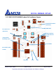
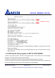
4.2 Kit PIN OUT
DELTA DFCE-NNN40 has a default profile pin out. The board has reserved SPI, I2C, ADC,
UART and GPIO pin to access. The following is the detail of description for pin out.
1.8V pin
The voltage of power supply for BLE module is 1.8V. All BT GPIO (P4~P29), are connected
to BLE SoC. It is notice that the voltage should be 1.8V.
3.6V pin
There are pins are passed through level shift to convert from 1.8V to 3.6V. Those are
SCL_3V6, SDA_3V6, STLK_TX, and STLK_RX.
RF switch pin
To switch RF antenna to BLE or Wi-Fi, it is controlled by gpio pin SWIO, P19.
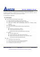
Use j-link to load image to BLE module directly
It is able to use j-link to load image to BLE module directly. The R124 and R125 should be
removed. The SWDIO and SWDCLK is then accessible on CN7 pin 25, 23 respectively.
ADC function
P04, P05, P06, P26, P27 could be to ADC function. It is notice that only P06 could be
configure to reference ADC voltage (ADC/LPCOMP reference input 0 and in input 1). Only
one of the modules can be enabled at the same time.