FEATURES High efficiency: 92% @ 12V/8A Size: 58.4mmx22.8mmx8.4mm (2.30”x0.90”x0.33”) (Without heat-spreader) 58.4mmx22.8mmx12.7mm (2.30”x0.90”x0.
LUO LUOTECHNICAL SPECIFICATIONS (TA=25°C, airflow rate=300 LFM, Vin=48Vdc, nominal Vout unless otherwise noted.) PARAMETER NOTES and CONDITIONS E48SC12008 (Standard) Min.
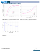
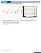
ELECTRICAL CHARACTERISTICS CURVES Figure 1: Efficiency vs. load current for 8A, minimum, nominal, and maximum input voltage at 25°C Figure 2: Power dissipation vs. load current for 8A, minimum, nominal, and maximum input voltage at 25°C.
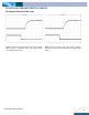
ELECTRICAL CHARACTERISTICS CURVES For Negative Remote On/Off Logic Figure 4: Turn-on transient at full rated load current (CC Mode load) (10ms/div). Vin=48V.Top Trace: Vout, 5V/div; Bottom Trace: ON/OFF input, 5V/div DS_E48SC12008_03192012 Figure 5: Turn-on transient at zero load current (10ms/div). Vin=48V.
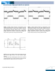
ELECTRICAL CHARACTERISTICS CURVES Figure 6: Output voltage response to step-change in load current (50%-25%-50% of Io, max; di/dt = 0.1A/µs). Load cap: 10µF, tantalum capacitor and 1µF ceramic capacitor. Top Trace: Vout (200mV/div, 200us/div), Bottom Trace: I out (2A/div). Scope measurement should be made using a BNC cable (length shorter than 20 inches).
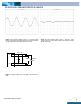
ELECTRICAL CHARACTERISTICS CURVES Figure 9: Input Terminal Ripple Current, ic, at full rated output current and nominal input voltage with 12µH source impedance and 33µF electrolytic capacitor (100mA/div,1us/div) Copper Figure 10: Input reflected ripple current, is, through a 12µH source inductor at nominal input voltage and rated load current (20mA/div,1us/div) Strip Vo(+) 10u 1u SCOPE RESISTIVE LOAD Vo(-) Figure 11: Output voltage noise and ripple measurement test setup DS_E48SC12008_03192012
ELECTRICAL CHARACTERISTICS CURVES 13.0 12.0 11.0 OUTPUT VOLTAGE(V) 10.0 9.0 8.0 7.0 6.0 5.0 4.0 3.0 2.0 1.0 0.0 0 Figure 12: Output voltage ripple at nominal input voltage and rated load current (Io=8A)(20mV/div,1us/div) Load capacitance: 1µF ceramic capacitor and 10µF tantalum capacitor. Bandwidth: 20 MHz. Scope measurements should be made using a BNC cable (length shorter than 20 inches).
DESIGN CONSIDERATIONS Input Source Impedance The impedance of the input source connecting to the DC/DC power modules will interact with the modules and affect the stability. A low ac-impedance input source is recommended. If the source inductance is more than a few μH, we advise adding a 10 to 100 μF electrolytic capacitor (ESR < 0.7 Ω at 100 kHz) mounted close to the input of the module to improve the stability.
FEATURES DESCRIPTIONS Vi(+) Vo(+) Over-Current Protection Sense(+) The modules include an internal output over-current protection circuit, which will endure current limiting for an unlimited duration during output overload. If the output current exceeds the OCP set point, the modules will automatically shut down (hiccup mode). The modules will try to restart after shutdown. If the overload condition still exists, the module will shut down again.
FEATURES DESCRIPTIONS (CON.) Output Voltage Adjustment (TRIM) To increase or decrease the output voltage set point, the modules may be connected with an external resistor between the TRIM pin and either the SENSE(+) or SENSE(-). The TRIM pin should be left open if this feature is not used.
THERMAL CONSIDERATIONS Thermal management is an important part of the system design. To ensure proper, reliable operation, sufficient cooling of the power module is needed over the entire temperature range of the module. Convection cooling is usually the dominant mode of heat transfer. Hence, the choice of equipment to characterize the thermal performance of the power module is a wind tunnel.
THERMAL CURVES (WITHOUT HEAT SPREADER) NTC RESISTOR THERMAL CURVES (WITH HEAT SPREADER) AIRFLOW AIRFLOW HOT SPOT 1 HOT SPOT 2 Figure 19: * Hot spot 1& NTC resistor temperature measured Figure 21: * Hot spot 2 temperature measured point points Output Current (A) 9.0 E48SC12008(Standard) Output Current vs. Ambient Temperature and Air Velocity @Vin = 48V (Transverse Orientation) Output Current (A) 9.0 E48SC12008(Standard) Output Current vs.
PICK AND PLACE LOCATION(SMD) RECOMMENDED PAD LAYOUT (SMD) SURFACE-MOUNT TAPE & REEL DS_E48SC12008_03192012 13
LEADED (Sn/Pb) PROCESS RECOMMEND TEMPERATURE PROFILE(SMD) Note: The temperature refers to the pin of E48SC, measured on the pin +Vout joint. LEAD FREE (SAC) PROCESS RECOMMEND TEMPERATURE PROFILE(SMD) Temp. Peak Temp. 240 ~ 245 ℃ 217℃ Ramp down max. 4℃/sec. 200℃ 150℃ Preheat time 100~140 sec. Time Limited 90 sec. above 217℃ Ramp up max. 3℃/sec. 25℃ Time Note: The temperature refers to the pin of E48SC, measured on the pin +Vout joint.
MECHANICAL DRAWING Surface-mount module Through-hole module All pins are copper alloy with tin plated over Nickel under plating.
MECHANICAL DRAWING(WITH HEAT-SPREADER) * For modules with through-hole pins and the optional heatspreader, they are intended for wave soldering assembly onto system boards; please do not subject such modules through reflow temperature profile. All pins are copper alloy with tin plated over Nickel under plating.
PART NUMBERING SYSTEM E 48 S Type of Input Number of Product Voltage Outputs E- Eighth Brick 48 36~75V S- Single C 120 08 N R Product Series Output Voltage Output Current ON/OFF Logic Pin Length/Type 120 - 12V 08 -8A N - Negative K – 0.110’’ F- RoHS 6/6 A- Standard Functions P - Positive N - 0.145” (Lead Free) H - with Heatspreader C- Improved E48SR series F A Option Code R - 0.170” Space - C - 0.181” RoHS 5/6 S - 0.189” T - 0.220” L - 0.