
1X9 SC Duplex Receptacle Transceiver Module Specification Sheet
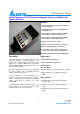

OPT-1250xxxx Series
DELTA ELECTRONICS, INC.
5 Jan., 2008
Rev. 0H
www.deltaww.com
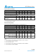
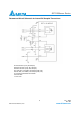
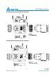
Pin Definition
PIN Symbol Functional description
1 GND Receiver Signal Ground
2 RD (+) Receiver Data Out Non-inverted (LVPECL)
3 RD (-) Receiver Data Out Inverted (LVPECL)
4 SD Receiver Signal Detect (LVPECL or TTL)
5 VccR Receiver Power Supply,
6 VccT Transmitter Power Supply
7 TD (-) Transmitter Data In Inverted (LVPECL)
8 TD (+) Transmitter Data In Non-inverted (LVPECL)
9 GND Transmitter Signal Ground
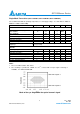
Pin Descriptions
Pin 1 Receiver Signal Ground, GND
Directly connect these pins to the ground plane.
Pin 2 Receiver Data Out Non-inverted (LVPECL), RD (+)
Receiver Data output Non-inverted (LVPECL), RD (+).
Pin 3 Receiver Data Out Inverted (LVPECL), RD (-)
Receiver Data output Inverted (LVPECL), RD (-).
Pin 4 Receiver Signal Detect (LVPECL/TTL), SD
PECL/TTL logic family. Normal Operation: Logic “1” Output
Fault Condition: Logic “0” Output.
Pin 5 Receiver Power Supply, VccR
Provide +3.3/5V dc power supply.
Pin 6 Transmitter Power Supply, VccT
Provide +3.3/5V dc power supply.
Pin 7 Transmitter Data In Inverted (LVPECL), TD (-)
Transmitter Data Input Inverted (LVPECL), TD (-)
Pin 8 Transmitter Data In Non-inverted (LVPECL), TD (+)
Transmitter Data Input Non-inverted (LVPECL), TD (+)
Pin 9 Transmitter Signal Ground, GND
Directly connect these pins to the ground plane.