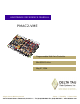
^1 HARDWARE REFERENCE MANUAL ^2 PMAC2-VME ^3 Programmable Multi-Axis Controller ^4 3Ax-602413-xHxx ^5 May 27, 2004 Single Source Machine Control Power // Flexibility // Ease of Use 21314 Lassen Street Chatsworth, CA 91311 // Tel. (818) 998-2095 Fax. (818) 998-7807 // www.deltatau.
Copyright Information © 2003 Delta Tau Data Systems, Inc. All rights reserved. This document is furnished for the customers of Delta Tau Data Systems, Inc. Other uses are unauthorized without written permission of Delta Tau Data Systems, Inc. Information contained in this manual may be updated from time-to-time due to product improvements, etc., and may not conform in every respect to former issues. To report errors or inconsistencies, call or email: Delta Tau Data Systems, Inc.
PMAC2 VME Hardware Reference Manual Table of Contents INTRODUCTION .......................................................................................................................................................1 Features .....................................................................................................................................................................1 PMAC2 VME Configuration ...........................................................................................
PMAC VME Hardware Reference Manual J3 ........................................................................................................................................................................35 J4 (JEXP)............................................................................................................................................................35 J5 (JTAG/OnCE) .......................................................................................................................
PMAC2 VME Hardware Reference Manual INTRODUCTION The PMAC2 VME provides state-of-the-art motion control for a wide variety of applications, including machine tools, robotics, semiconductor manufacturing, packaging equipment, and general-purpose automation. It utilizes the latest developments in electronics, software, and modern control theory to bring motion control capabilities to a whole new level. The PMAC2 VME is designed as a bus expansion card, but is capable of standalone operation.
PMAC VME Hardware Reference Manual • • • • Amplifier fault input Four supplementary flag inputs (T, U, V, W) Two inputs from serial analog-to-digital converters (ADCs) ADC clock and strobe signal outputs The DSPGATE1 ASIC also generates several clock frequencies necessary for hardware and software operation, under the user’s software control: • PWM output frequency • DAC clock frequency • ADC clock frequency • Encoder sample clock frequency • Pulse-frequency modulation (PFM) clock frequency • Phase interru
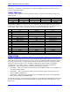
PMAC2 VME Hardware Reference Manual Alternately, you can define an M-variable such as M99->X:$FFFD,0,4 and then read from or write to these bits with the M-variable. PMAC2 VME Setup On PMAC2 VME, jumpers E2 and E4 control the frequency of operation of the DSP according to the following table: E2 E4 X:$FFFD; 0-3 True Multiplier DSP Frequency OFF ON OFF OFF OFF ON 1 2 3 x2 x3 x4 40 MHz 60 MHz 80 MHz On the PMAC2 VME, I54 is read at power-up to set the baud rate clock.
PMAC VME Hardware Reference Manual The PV CPU has operational differences from earlier CPU configurations to support the new features. The following paragraphs explain these differences and are only relevant if using the 602705 CPU piggyback board on the controller. Configurations The PV CPU board is configured at the factory to the customer’s specifications. The JEXP expansion port is buffered, providing the capability to connect many boards on the expansion port.
PMAC2 VME Hardware Reference Manual Any value written into the Option 16 memory will automatically be retained through a power-down or reset; no SAVE operation is required. The power draw on the battery is low enough that battery life will typically be limited only by the quoted 10-year life of the battery.
PMAC VME Hardware Reference Manual 6 Introduction
PMAC2 VME Hardware Reference Manual CONNECTORS PMAC2 VME Connector Summary The following paragraphs provide a brief description of each connector on the PMAC2 VME, its use, and individual pinout information.
PMAC VME Hardware Reference Manual 19 J1/JANA (20-Pin Header) 1 20 2 Front View Pin # Symbol Function Description Notes 1 ANAI00 Input Analog Input 0 0-5V or +/-2.5V range 2 ANAI01 Input Analog Input 1 0-5V or +/-2.5V range 3 ANAI02 Input Analog Input 2 0-5V or +/-2.5V range 4 ANAI03 Input Analog Input 3 0-5V or +/-2.5V range 5 ANAI04 Input Analog Input 4 0-5V or +/-2.5V range 6 ANAI05 Input Analog Input 5 0-5V or +/-2.5V range 7 ANAI06 Input Analog Input 6 0-5V or +/-2.
PMAC2 VME Hardware Reference Manual J2/JTHW (26-Pin Header) Front View Pin # Symbol Function Description Notes 1 GND Common PMAC Common 2 GND Common PMAC Common 3 DAT0 Input Data-0 Input Data Input from Mux Port Accessories 4 SEL0 Output Select-0 Output Address/Data Output for Mux Port Accessories 5 DAT1 Input Data-1 Input Data Input from Mux Port Accessories 6 SEL1 Output Select-1 Output Address/Data Output for Mux Port Accessories 7 DAT2 Input Data-2 Input Data Input from Mux Port Accessories 8 SEL
PMAC VME Hardware Reference Manual J3/JIO (40-Pin Header) 39 40 1 2 Front View Pin # Symbol Function Description Notes 1 I/O00 In/Out Digital I/O 0 Software direction ctrl. 2 I/O01 In/Out Digital I/O 1 Software direction ctrl. 3 I/O02 In/Out Digital I/O 2 Software direction ctrl. 4 I/O03 In/Out Digital I/O 3 Software direction ctrl. 5 I/O04 In/Out Digital I/O 4 Software direction ctrl. 6 I/O05 In/Out Digital I/O 5 Software direction ctrl. 7 I/O06 In/Out Digital I/O 6 Software direction ctrl.
PMAC2 VME Hardware Reference Manual J4 (JMACRO) 26-Pin Header Front View Pin # Symbol Function Description Notes 1 DOUT7 Output Ring Out Bit 7 Macro Ring Command 2 DOUT6 Output Ring Out Bit 6 Macro Ring Transmit 3 DOUT5 Output Ring Out Bit 5 Macro Ring Transmit 4 DOUT4 Output Ring Out Bit 4 Macro Ring Transmit 5 DOUT3 Output Ring Out Bit 3 Macro Ring Transmit 6 DOUT2 Output Ring Out Bit 2 Macro Ring Transmit 7 DOUT1 Output Ring Out Bit 1 Macro Ring Transmit 8 DOUT0 Output Ring Out Bit 0 Macro Ring Tr
PMAC VME Hardware Reference Manual J5A/JRS422 (26-Pin Header) Front View Pin # Symbol Function Description Notes 1 CHASSI Common PMAC Common 2 S+5V Output +5Vdc Supply 3 RDInput Receive Data Diff. I/O Low True ** 4 RD+ Input Receive Data Diff. I/O High True * 5 SDOutput Send Data Diff. I/O Low True ** 6 SD+ Output Send Data Diff. I/O High True * 7 CS+ Input Clear to Send Diff. I/O High True ** 8 CSInput Clear to Send Diff. I/O Low True * 9 RS+ Output Req. to Send Diff.
PMAC2 VME Hardware Reference Manual J6/JDISP (14-Pin Header) Front View Pin # Symbol Function Description Notes 1 VDD Output +5V Power Power Supply Out 2 VSS Common PMAC Common 3 RS Output Read Strobe TTL Signal Out 4 VEE Output Contrast Adjust VEE 0 to +5Vdc * 5 E Output Display Enable High is Enable 6 R/W Output Read Or Write TTL Signal Out 7 DB1 Output Display Data1 8 DB0 Output Display Data0 9 DB3 Output Display Data3 10 DB2 Output Display Data2 11 DB5 Output Display Data5 12 DB4 Output Display D
PMAC VME Hardware Reference Manual J8/JEQU (10-Pin Header) Front View Pin # Symbol Function Description Notes 1 EQU1/ Output Enc. 1 Comp-Eq Low is true 2 EQU2/ Output Enc. 2 Comp-Eq Low is true 3 EQU3/ Output Enc. 3 Comp-Eq Low is true 4 EQU4/ Output Enc. 4 Comp-Eq Low is true 5 EQU5/ Output Enc. 5 Comp-Eq Low is true 6 EQU6/ Output Enc. 6 Comp-Eq Low is true 7 EQU7/ Output Enc. 7 Comp-Eq Low is true 8 EQU8/ Output Enc.
PMAC2 VME Hardware Reference Manual J9/JMACH1 (100-Pin Header) 99 100 1 2 Front View Pin# 33 34 35 Symbol Function Notes Programmable polarity 47 48 49 FAULT1+ FAULT1PWMATOP1+ DAC_CLK1+ PWMATOP1DAC_CLK1PWMABOT1+ DAC1A+ PWMABOT1DAC1APWMBTOP1+ DAC_STB1+ PWMBTOP1DAC_STB1PWMBBOT1+ DAC1B+ PWMBBOT1DAC1BPWMCTOP1+ DIR1+ PWMCTOP1DIR1PWMCBOT1+ PULSE1+ PWMCBOT1PULSE1GND GND +5V Common Common Output / Input Amplifier Fault Amplifier Fault Phase A Top CMD or DAC Clock Phase A Top CMD or DAC Clock Phase A Bot
PMAC VME Hardware Reference Manual J9/JMACH1 (100-Pin Header) 99 100 1 2 Front View Pin# Symbol Function Description Notes For loss of ACC supply voltage Low is PMAC watchdog fault Direction controlled by PMAC2 jumper 69 70 71 ACCFLT2 WD0/ SCLK12+ Input Output Input / Output Accessory Fault Flag Watchdog Output Encoder Sample Clock 72 73 74 75 76 77 78 79 80 81 82 83 84 85 SCLK12ADC_CLK2+ ADC_CLK2ADC_STB2+ ADC_STB2ADC_DAA2+ ADC_DAA2ADC_DAB2+ ADC_DAB2AENA2+ AENA2FAULT2+ FAULT2PWMATOP2+ DAC_CLK
PMAC2 VME Hardware Reference Manual J10/JMACH2 (100-Pin Header) 99 100 1 2 Front View Pin# Symbol Function Description Notes 1 +5V Output / Input +5V Power For external circuit or from ext. Supply 2 3 4 5 6 7 8 9 10 11 +5V GND GND CHA3+ CHA3CHB3+ CHB3CHC3+ CHC3CHU3 Output / Input Common Common Input Input Input Input Input Input Input +5V Power Reference Voltage Reference Voltage Enc 3 Pos. A Chan. Enc 3 Neg. A Chan. Enc 3 Pos. B Chan. Enc 3 Neg. B Chan. Enc 3 Pos. C Chan. Enc 3 Neg.
PMAC VME Hardware Reference Manual J10/JMACH2 (100-Pin Header) 99 100 1 2 Front View Pin# Symbol Function 40 Output 47 48 49 PWMBTOP3DAC_STB3PWMBBOT3+ DAC3B+ PWMBBOT3DAC3BPWMCTOP3+ DIR3+ PWMCTOP3DIR3PWMCBOT3+ PULSE3+ PWMCBOT3PULSE3GND GND +5V Common Common Output / Input Phase B Top CMD or DAC Strobe Phase B Bottom CMD or DAC B Serial Data Phase B Bottom CMD or DAC B Serial Data Phase B Top CMD or PFM Direction Phase B Top CMD or PFM Direction Phase B Bottom CMD or PFM Pulse Phase B Bottom CMD
PMAC2 VME Hardware Reference Manual J10/JMACH2 (100-Pin Header) 99 100 1 2 Front View Pin# 76 77 78 79 80 81 82 83 84 85 86 87 88 89 90 91 92 93 94 95 96 97 98 99 Symbol Function ADC_STB4Output ADC_DAA4+ Input ADC_DAA4Input ADC_DAB4+ Input ADC_DAB4Input AENA4+ Output AENA4Output FAULT4+ Input FAULT4Input PWMATOP4+ Output DAC_CLK4+ PWMATOP4Output DAC_CLK4PWMABOT4+ Output DAC4A+ PWMABOT4Output DAC4APWMBTOP4+ Output DAC_STB4+ PWMBTOP4Output DAC_STB4PWMBBOT4+ Output DAC4B+ PWMBBOT4- Output DAC4BPWMCTOP4
PMAC VME Hardware Reference Manual P1 JMACH (96-Pin Header) Front View Pin # Row A Row B Row C 01 D00 BBSY/ D08 02 D01 BCLR/ D09 03 D02 ACFAIL/ D10 04 D03 B0IN/ D11 05 D04 BG0OUT/ D12 06 D05 BG1IN/ D13 07 D06 BG1OUT/ D14 08 D07 BG2IN/ D15 09 GND BG2OUT/ GND 10 SYSCLK BG3IN/ SYSFAIL/ 11 GND BG3OUT/ BERR/ 12 DS1/ BR0/ SYSRESET/ 13 DS0/ BR1/ LWORD/ 14 WRITE/ BR2/ AM5 15 GND BR3/ A23 16 DTACK/ AM0 A22 17 GND AM1 A21 18 AS/ AM2 A20 19 GND AM3 A19 20 IACK/ GND A18 21 IACKIN/ SERCLK A17 22 IACKOUT/ SERDAT/ A
PMAC2 VME Hardware Reference Manual P2/JMACHA (96-Pin Header) Front View Pin# Row A Row B (Format A) Row B (Format B) Row C 01 02 03 04 05 06 07 08 09 10 11 +5V +5V CHU1 +5V GND GND CHU3 GND CHA1 (Reserved) CHV1 CHA3 CHB1 VA24 CHV3 CHB3 CHC1 VA25 CHW1 CHC3 PLIM1 VA26 CHW3 PLIM3 MLIM1 VA27 CHT1 MLIM3 HOME1 VA28 CHT3 HOME3 AENA1 VA29 USER1 AENA3 FAULT1 VA30 USER3 FAULT3 PWMATOP1/ VA31 ADC_DAA1 PWMATOP3/ DAC_CLK1 DAC_CLK3 12 PWMABOT1/ DAC1A GND ADC_DAA3 PWMABOT3/ DAC3A 13 PWMBTOP1/ +5V ADC_DAB1 PWMBTOP
PMAC VME Hardware Reference Manual TB1 (2/4-Pin Terminal Block) Pin# Symbol Function Description 1 2 3 GND +5V +12V Common Input Input Reference Voltage Positive Supply Voltage Positive Supply Voltage Notes Supplies all PMAC digital circuits +12v to +15v; not required on-board; used on j1 to supply analog inputs 4 -12V Input Negative Supply Voltage -12V to –15V; required for Opt-12 ADCs; used on J1 to supply analog inputs This terminal block can be used to provide the input for the power supply fo
PMAC2 VME Hardware Reference Manual JUMPER SUMMARY See PMAC2 VME layout diagram for jumper locations. E1: Card 0 Select E Point and Physical Layout Location E1 B1 Description Remove jumper to specify that this is Card 0, which generates its own phase and servo clock (default). Jump pins 1 to 2 to specify that this is not card 0, but Card 1 to F (15), which requires external phase and servo clock signals from the serial port to operate.
PMAC VME Hardware Reference Manual E7A-H through E10A-H: P2 Connector B-Row Use Select E Point and Physical Layout Location Description Jump pins 1 to 2 to use B-row of P2 connector for JMACH pins (not compatible with 32-bit VME). Jump pins 2 to 3 to use B-row of P2 connector for 32bit VME bus interface B5 Jump pins 1 to 2 to use B-row of P2 connector for E8A-H JMACH pins (not compatible with 32-bit VME).
PMAC2 VME Hardware Reference Manual E17 - E18: Serial Connector Select E17 and E18 control whether the RS-232 or RS-422 serial port is used. E Point and Physical Layout Location Description Default E17 B2 Jump pins 1 to 2 to use RS-232 serial interface. Jump pins 2 to 3 to use RS -422 serial interface 1-2 jumper installed E18 C2 Jump pins 1 to 2 to use RS -232 serial interface.
PMAC VME Hardware Reference Manual Option 1V Piggyback Connector Description The following paragraphs provide a brief description of each connector on the Option 1V Piggyback card, its use, and individual pinout information (see Figure 2-2).
PMAC2 VME Hardware Reference Manual 99 100 J11/JMACH3 (100-Pin Header) 1 2 Front View Pin# Symbol 25 26 27 28 29 30 31 32 33 34 35 ADC_STB5+ ADC_STB5ADC_DAA5+ ADC_DAA5ADC_DAB5+ ADC_DAB5AENA5+ AENA5FAULT5+ FAULT5PWMATOP5+ DAC_CLK5+ PWMATOP5DAC_CLK5PWMABOT5+ DAC5A+ PWMABOT5DAC5APWMBTOP5+ DAC_STB5+ PWMBTOP5DAC_STB5PWMBBOT5+ DAC5B+ PWMBBOT5DAC5BPWMCTOP5+ DIR5+ PWMCTOP5DIR5PWMCBOT5+ PULSE5+ PWMCBOT5PULSE5GND GND +5V +5V +5V +5V GND GND CHA6+ CHA6CHB6+ CHB6CHC6+ CHC6CHU6 CHV6 36 37 38 39 40 41 42 43 44 4
PMAC VME Hardware Reference Manual 99 100 J11/JMACH3 (100-Pin Header) 1 2 Front View Pin# Symbol 63 64 65 66 67 68 69 70 71 72 73 74 75 76 77 78 79 80 81 82 83 84 85 CHW6 CHT6 USER6 PLIM6 MLIM6 HOME6 ACCFLT6 WD0/ SCLK56+ SCLK56ADC_CLK6+ ADC_CLK6ADC_STB6+ ADC_STB6ADC_DAA6+ ADC_DAA6ADC_DAB6+ ADC_DAB6AENA6+ AENA6FAULT6+ FAULT6PWMATOP6+ DAC_CLK6+ PWMATOP6DAC_CLK6PWMABOT6+ DAC6A+ PWMABOT6DAC6APWMBTOP6+ DAC_STB6+ PWMBTOP6DAC_STB6PWMBBOT6+ DAC6B+ PWMBBOT6DAC6BPWMCTOP6+ DIR6+ PWMCTOP6DIR6PWMCBOT6+ PULSE6+ P
PMAC2 VME Hardware Reference Manual 98 GND Common Reference Voltage 99 +5V Output / Input +5v Power For external circuit or from external supply 100 +5V Output / Input +5v Power The JMACH3 connector provides the interface pins for channels 5 and 6. It is usually connected to a breakout board, such as one of the Acc-8x family of boards, or an application-specific interface board. Note: 100-pin male box header with center key, 0050 pitch. AMP part # 1-04068-7. Delta Tau part # 014-00010-FPB.
PMAC VME Hardware Reference Manual J12/JMACH4 (100-Pin Header) 99 100 1 2 Front View Pin# Symbol 39 PWMBTOP7+ DAC_STB7+ PWMBTOP3DAC_STB7PWMBBOT7+ DAC7B+ PWMBBOT7DAC7BPWMCTOP7+ DIR7+ PWMCTOP7DIR7PWMCBOT7+ PULSE7+ PWMCBOT7PULSE7GND GND +5V +5V +5V +5V GND GND CHA8+ CHA8CHB8+ CHB8CHC8+ CHC8CHU8 CHV8 CHW8 CHT8 USER8 PLIM8 MLIM8 HOME8 ACCFLT8 WD0/ SCLK78+ SCLK78ADC_CLK8+ ADC_CLK8ADC_STB8+ ADC_STB8ADC_DAA8+ ADC_DAA8ADC_DAB8+ ADC_DAB8- 40 41 42 43 44 45 46 47 48 49 50 51 52 53 54 55 56 57 58 59 60 61 62 6
PMAC2 VME Hardware Reference Manual J12/JMACH4 (100-Pin Header) 99 100 1 2 Front View Pin# Symbol Function Description Notes 81 82 83 84 85 AENA8+ Output Amplifier Enable High is enable AENA8Output Amplifier Enable Low is enable FAULT8+ Input Amplifier Fault Programmable polarity FAULT8Input Amplifier Fault PWMATOP8+ Output Phase A Top CMD or DAC Programmable function control DAC_CLK8+ Clock 86 PWMATOP8- Output Phase A Top CMD or DAC DAC_CLK8Clock 87 PWMABOT8+ Output Phase A Bottom CMD or DAC Pro
PMAC VME Hardware Reference Manual P2A/JMACHB (96-Pin Header) Front View Pin# Row A Row B (Format A) Row B (Format B) Row C 01 02 03 04 05 06 07 08 09 10 11 +5V No Connect CHU5 +5V GND No Connect CHU7 GND CHA5 No Connect CHV5 CHA7 CHB5 No Connect CHV7 CHB7 CHC5 No Connect CHW5 CHC7 PLIM5 No Connect CHW7 PLIM7 MLIM5 No Connect CHT5 MLIM7 HOME5 No Connect CHT7 HOME7 AENA5 No Connect USER5 AENA7 FAULT5 No Connect USER7 FAULT7 PWMATOP5/ No Connect ADC_DAA5 PWMATOP7/ DAC_CLK5 DAC_CLK7 12 PWMABOT5/ DAC5A
PMAC2 VME Hardware Reference Manual OPTION 1V PIGGYBACK JUMPER SUMMARY See the Option 1V Piggyback board layout diagram for jumper locations. E Point and Physical Layout Location Description Default Jump pins 1 to 2 to use B-row of P2A connector for 1-2 jumpers installed JMACH pins (not compatible with 32-bit VME). Remove jumpers to leave B-row of P2A unconnected to prevent contention with 32-bit VME Bus.
PMAC VME Hardware Reference Manual 34 Option 1V Piggyback Jumper Summary
PMAC2 VME Hardware Reference Manual PMAC2 VME CPU Connector Summary The following paragraphs provide a brief description of each connector on the PMAC2 VME CPUs. J1 35 36 ` 1 2 Front View 36-pin header on backside for connection to main PMAC/PMAC2 board. J2 (JEXP) 49 50 1 2 Front View 50-pin IDC header for connection to expansion port accessory boards. J3 35 36 ` 1 2 Front View 36-pin header on backside for connection to main PMAC/PMAC2 board.
PMAC VME Hardware Reference Manual P/N 602405 J3 (OTHER SIDE) PMAC2 VME CPU Board P/N 602705 36 PMAC2 VME CPU
PMAC2 VME Hardware Reference Manual PMAC2 VME CPU Piggyback Board Jumpers See the PMAC PC CPU Piggyback Board layout diagram for jumper locations. E Point and Physical Layout Location Description Default E1 D1 (602398) A1 (602405) B1 (602705) Remove jumper to enable watchdog timer operation. Jump pins 1 to 2 to disable watchdog timer operation (for test purposes only).