
Specifications
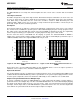

1st stage
of ÐÂ
Modulator
V
IN
+
V
IN
-
ADC
Differential
Input p
Differential
Input n
R
EXT
R
EXT
ADC12EU050
SNAS444I –JANUARY 2008–REVISED APRIL 2013
www.ti.com
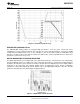
The ADC12EU050 internally generates a common mode of 0.62V. It is possible to provide input signals with
other common modes however, the full scale input range of the ADC must be kept in mind.
For this reason, it is recommended that the device inputs are AC coupled. The recommended capacitor value is
100nF.
External Series Resistance
Due to the purely resistive input circuit of the sigma delta architecture, the ADC12EU050 allows the user to scale
down large input signals by adding external series resistors. The gain achieved by adding external resistors can
be calculated as a simple voltage divider, as follows:
V
FS
/V
IN
= 20 * log (R
ADC
/( R
ADC
+ R
EXT
)) dB (1)
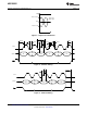
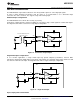
The diagram below shows this configuration, and defines the values in the equation above.
Figure 16. External Series Resistance
R
ADC
, the input resistance of the ADC, is nominally 1.3kΩ. Due to manufacturing the value of this resistance can
vary by up to 15%. This is not important for the operation of the ADC, since the ADC depends only on internal
resistors being matched, but it should be taken into account when performing calculations.
ADC OUTPUT CONSIDERATIONS
The ADC12EU050 offers a variety of output settings in order to cater for different system design and integration
needs.
Output Driver Voltage, VDR
The ADC output driver voltage, VDR, can be set between 1.2V and 1.8V. A VDR of 1.2V will offer the lowest
power consumption. Because VDR can be varied, the ADC12EU050 provides, via the SPI registers, the ability to
adjust the output common mode voltage.
Output Modes And Output Common Mode
Three different output modes are also supported: SLVS, LVDS and reduced common mode LVDS. SLVS and
LVDS modes output data according to their respective specifications.
Reduced common mode LVDS must be used when the output driver voltage, VDR, is 1.2V. The standard LVDS
common mode voltage is 1.2V, which is obviously not feasible if VDR is 1.2V. Therefore, the output common
mode voltage must be set to 1.0V by setting the bit OCM in the LVDS Control Register to 0.
20 Submit Documentation Feedback Copyright © 2008–2013, Texas Instruments Incorporated
Product Folder Links: ADC12EU050