
User's Manual

Warning
Please read this instruction sheet carefully before use.
DO NOT touch any terminal when the power is switched on. Switch off the power before wiring.
DVP06XA-S is an OPEN-TYPE device and therefore should be installed in an enclosure free of airborne dust,
humidity, electric shock and vibration. The enclosure should prevent non-maintenance staff from operating the
device (e.g. key or specific tools are required to open the enclosure) in case danger and damage on the device may
occur.
DO NOT connect input AC power supply to any of the I/O terminals; otherwise serious damage may occur. Check all
the wiring again before switching on the power.
DO NOT touch the internal circuit for 1 minute after the power is switched off.
Make sure the ground terminal is correctly grounded in order to prevent electromagnetic interference.
Introduction
Model Explanation & Peripherals
Thank you for choosing Delta DVP series PLC. DVP06XA-S is able to receive 4 points of analog input
signals (voltage or current) and convert them into 12-bit digital signals. DVP06XA-S receives 2 groups of
12-bit digital data from the PLC MPU and converts them into 2 points of analog signals for output (in
voltage/current). There are 49 16-bit control registers (CR) in DVP06XA-S, and the data in it can be read
and written by using FROM/TO instructions in DVP Slim series PLC MPU program.
The system version of DVP06XA-S can be updated via RS-485 communication. The power unit is
separate from it and is small in size and easy to install.
The user can select voltage or current input by wiring. Range of voltage input: 10V DC (resolution: 5mV).
Range of current input: 20mA (resolution: 20µA).
The user can also select voltage or current output by wiring. Range of voltage output: 0V ~ +10V DC
(resolution: 2.5mV). Range of current output: 0mA ~ 20mA (resolution: 5µA).
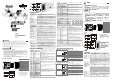
Product Profile & Outline
1.
Status indicator (POWER, RUN and
ERROR)
2.
Model
3.
DIN rail clip
4.
I/O terminals
5.
I/O terminals layout
6.
Expansion hole of the expansion unit
7.
Specification label
8.
Expansion port
9.
Expansion clip
10.
DIN rail location (35mm)
11.
RS-485 communication port
12.
Expansion clip
13.
DC power input
90.00
4.00
3.00
25.20
1
2
3
4
60.00
5
6
7
8
9
3
10
11
12
13
3.4
90.00
60.00
3.00
14
V+
I+
COM
C
H
1
V+
I+
COM
C
H
2
V+
I+
COM
C
H
3
V+
I+
COM
C
H
5
V+
I+
COM
C
H
6
V+
I+
COM
C
H
4
IN
OUT
Unit: mm
14.
Expansion port
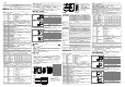
External Wiring
CH1
104 .7K
250
-10 V~+ 10V
V+
I+
COM
CH1
104 .7K
CH4
104 .7K
250
-20 mA~+ 20mA
V+
I+
COM
CH4
104 .7K
*3
*2
AG
AG
Current input
Voltage input
Shielded*1
Shielded*1
Note 1: Please isolate analog input and other
power wiring.
Note 2: If input signal is in current, please short
out between V+ and I+ terminals.
Note 3: If the noise interference from loaded
input wiring terminal is significant,
please connect a capacitor with 0.1 ~
0.47µF 25V for noise filtering.
ENGLISH
V+
I+
COM
CH5
0V~+10V
*5
CH5
V+
I+
COM
CH6
0mA~20mA
CH6
24+
24-
DC24V
DC/DC
+15V
-15V
AG
volt age outpu t
current output
AC drive, recorder,
scale valve.. .
shiel ding cable *1
shie lding cable *4
AC drive, recorder,
scale valve.. .
termin al of
power module
class 3 grounding
(100
or less)
convert er
DVP06XA-S
V+
I+
COM
V+
I+
COM
I+
COM
V+
I+
COM
V+
V+
I+
COM
V+
I+
COM
Note 4: Please isolate analog output and other
power wiring.
Note 5: If the noise interference from loaded
input wiring terminal is significant,
please connect a capacitor with 0.1 ~
0.47µF 25V for noise filtering.
Note 6: Please connect power module
terminal and analog output module
terminal to system earth point and make
system earth point be grounded or
connects to machine cover.
Warning: DO NOT wire to the No function
terminal .
Specifications
Mixed analog/digital (A/D)
module
Voltage input Current input
Power supply voltage 24V DC (20.4V DC ~ 28.8V DC) (-15% ~ +20%)
Analog input channel 4 channels per module
Analog input range ±10V ±20mA
Digital data range ±2,000 ±1,000
Resolution 12 bits (1
LSB
=5mV) 11 bits (1
LSB
=20µA)
Input impedance 200KΩ and above 250Ω
Overall accuracy ±0.5% of full scale of 25°C (77°F). ±1% of full scale during 0 ~ 55°C (32 ~ 131°F).
Response time 3ms × channels
Isolation method There is no isolation between channels
Absolution input range ±15V ±32mA
Digital data format 2’s complement of 16-bit, (13 significant bits)
Average function Yes (CR#2 ~ CR#5 can be set and the range is K1 ~ K4,095)
Self diagnostic function self
detection
Upper bound and lower bound detection per channel
Mixed digital/analog (D/A)
module
Voltage input Current input
Analog signal output channels 2 channel per module
Analog output range 0 ~ 10V 0 ~ 20mA
Digital data range 0 ~ 4,000 0 ~ 4,000
Resolution 12 bits (1
LSB
=2.5mV) 12 bits (1
LSB
=5µA)
Output impedance 0.5Ω or lower
Overall accuracy ±0.5% of full scale of 25°C (77°F). ±1% of full scale during 0 ~ 55°C (32 ~ 131°F).
Response time 3ms × channels
Max. output current 20mA (1KΩ ~ 2MΩ)
Tolerance carried impedance 0 ~ 500Ω
Digital data format 2’s complement of 16-bit, (13 significant bits).
Isolation method Isolation between digital and analog circuitry. There is no isolation between channels.
Protection
Voltage output has short circuit protection but long period of short circuit may cause
internal wiring damage and current output break.
Communication mode
(RS-485)
MODBUS ASCII/RTU Mode. Communication baud rate of 4,800/9,600/19,200/38,400
/57,600/115,200. For ASCII mode, date format is 7 bits, even, 1 stop bit (7, E, 1). For
RTU mode, date format is 8 bits, even, 1 stop bit (8, E, 1). The RS-485 is disabled
when the DVP06XA-S is connected in series with MPU.
Connect to DVP-PLC MPU
in series
When DVP06XA-S modules are connected to an MPU, the modules are numbered
from 0-7. 0 is the closest to the MPU and 7 is the furthest. The Maximum number of
modules is 8 modules and they do not occupy any digital I/O points of the MPU.
Others
Power
supply
Maximum power consumption 2W at 24V DC (20.4V DC ~ 28.8V DC) (-15% ~ +20%), supplied by external power.
Environment
Operation/storage
Operation: 0°C ~ 55°C (temperature); 50 ~ 95% (humidity); pollution degree 2.
Storage: -25°C ~70°C (temperature); 5 ~ 95% (humidity).
Vibration/shock immunity
International standards: IEC 61131-2, IEC 68-2-6 (TEST Fc)/IEC 61131-2 & IEC
68-2-27 (TEST Ea)
CR (Control Register)
b15
b14
b13
b12
b11
b10
b9
b8
b7
b6
b5
b4
b3
b2
b1
b0
CR
#
RS-485
parameter
address
Latched
Register name
CH6 CH5 CH4 CH3 CH2 CH1
#0
H’40C8
○
R
Model type
System used, data length is 8 bits (b7 ~ b0). DVP06XA-S model code
= H’CC
#1
H’40C9
○
R/W
Input mode setting
Input mode setting: (CH1 ~ CH4)
Mode 0: input voltage mode (-10V ~ +10V).
Mode 1: input voltage mode (-6V ~ +10V). Mode 2: input current mode
(-12mA ~ +20mA). Mode 3: input current mode (-20Ma ~ +20mA).
Mode 4: none use.
Output mode setting: (CH5 ~ CH6)
Mode 0: output voltage mode (0V ~ 10V). Mode 1: output voltage mode
(2V ~ 10V). Mode 2: output current mode (4mA ~ 20mA). Mode 3:
output current mode (0mA ~ 20mA).
CR#1: b11 ~ b0 are used to set 4 internal channels working mode of analog input module (AD). b12 ~ b15 are used to set
2 channels working mode of analog output module (DA). Every channel has four modes that can be set individually. For
example: if setting CH1 to mode 0 (b2 ~ b0=000), CH2 to mode 1 (b5 ~ b3=001), CH3: mode 2 (b8 ~ b6=010), CH4:
mode 3 (b11 ~ b9=011), b0 ~ b11 need be set to H’688. If setting CH5: mode 2 (b13 ~ b12=10), CH6: mode 1 (b15 ~
b14=01), b12 ~ b15 need be set to H’5. Factory Setting is H’0000.
#2
H’40CA
○
R/W
CH1 average number
#3
H’40CB
○
R/W
CH2 average number
#4
H’40CC
○
R/W
CH3 average number
#5 H’40CD
○
R/W
CH4 average number
The number of readings used for “average” temperature on channels
CH1 ~ CH4. Setting range is K1 ~ K4,095 and factory setting is K10.
#6
H’40CE
R
Average value of CH1
input signal
#7
H’40CF
R
Average value of CH2
input signal
#8
H’40D0
R
Average value of CH3
input signal
#9
H’40D1
R
Average value of CH4
input signal
Display average value of CH1 ~ CH4 input signal.
Example: If CR#2 is 10, the temperature in CR#6 will be the average of
the last 10 readings on CH1.
#10
H’40D2
R/W
CH5 output signal value
#11
H’40D3
R/W
CH6 output signal value
Output value of CH5 ~ CH6, the setting range is K0 ~ K4,000. The
factory setting is K0 and the unit is LSB.
#12
H’40D4
R
Present value of CH1
input signal
#13
H’40D5
R
Present value of CH2
input signal
#14
H’40D6
R
Present value of CH3
input signal
#15
H’40D7
R
Present value of CH4
input signal
Display present value of CH1 ~ CH4 input signal
#18
H’40DA
○
R/W
To adjust OFFSET
value of CH1
#19
H’40DB
○
R/W
To adjust OFFSET
value of CH2
Offset setting of CH1 ~ CH4. Factory setting is K0 and unit is LSB.
b15
b14
b13
b12
b11
b10
b9
b8
b7
b6
b5
b4
b3
b2
b1
b0
CR
#
RS-485
parameter
address
Latched
Register name
CH6 CH5 CH4 CH3 CH2 CH1
#20
H’40DC
○
R/W
To adjust OFFSET
value of CH3
#21
H’40DD
○
R/W
To adjust OFFSET
value of CH4
Voltage input: setting range is K-1,000
LSB
~ K1,000
LSB
.
Current input: setting range is K-1,000
LSB
~ K1,000
LSB
.
#22
H’40DE
○
R/W
To adjust OFFSET
value of CH5
#23
H’40DF
○
R/W
To adjust OFFSET
value of CH6
Offset setting of CH5 ~ CH6. Factory setting is K0 and unit is LSB.
The setting range is K-2,000
LSB
~ K2,000
LSB
.
#24
H’40E0
○
R/W
To adjust GAIN value of
CH1
#25
H’40E1
○
R/W
To adjust GAIN value of
CH2
#26
H’40E2
○
R/W
To adjust GAIN value of
CH3
#27
H’40E3
○
R/W
To adjust GAIN value of
CH4
GAIN setting of CH1 ~ CH4. Factory setting is K1,000 and unit is LSB.
Voltage input: setting range is K-800
LSB
~ K4,000
LSB
.
Current input: setting range is K-800
LSB
~ K2,600
LSB
.
Please be notice that GAIN VALUE - OFFSET VALUE=+200
LSB
~
+3,000
LSB
(voltage) or +200
LSB
~ +1,600
LSB
(current)
#28
H’40E4
○
R/W
To adjust GAIN value of
CH5
#29
H’40E5
○
R/W
To adjust GAIN value of
CH6
GAIN setting of CH5 ~ CH6. Factory setting is K2,000 and unit is LSB.
The setting range is K0 ~ K4,000.
Please be noticed that GAIN value – OFFSET value= +400
LSB
~
+6,000
LSB
(voltage or current).
CR#24~CR#29: If the value difference comes up small (within range), the output signal resolution is then slim and the
variation is definitely larger. On the contrast, if the value difference exceeds the range, the output signal resolution
becomes larger and the variation is definitely smaller.
#30
H’40E6
R
Error status Data register stores the error status, see error code chart for details.
CR#30 is the error code. Please refer to the chart below.
Error description Content b15 ~ b8
b7
b6
b5
b4
b3
b2
b1
b0
Power source abnormal (low voltage alarm)
K1 (H’1) 0 0 0 0 0 0 0 1
User setting D/A output exceeds range K2 (H’2) 0 0 0 0 0 0 1 0
Setting mode error K4 (H’4) 0 0 0 0 0 1 0 0
Offset/gain error K8 (H’8) 0 0 0 0 1 0 0 0
Hardware malfunction K16 (H’10) 0 0 0 1 0 0 0 0
Digital range error K32 (H’20) 0 0 1 0 0 0 0 0
Average times setting error K64 (H’40) 0 1 0 0 0 0 0 0
Instruction error K128 (H’80)
Reserved
1 0 0 0 0 0 0 0
Note: Each error code will have corresponding bit (b0 ~ b7). Two or more errors may happen at the same time. 0 means normal
and 1 means having error.
EX: if the digital input exceeds 4,000, error (K2) will occur. If the analog output exceeds 10V, both analog input value
error K2 and K32 will occur. (A/D does not support displaying error K2.)
#31
H’40E7
○
R/W
Communication
address setting
RS-485 communication address.
Setting range is K1 ~ K254 and factory setting is K1.
#32
H’40E8
○
R/W
Communication baud
rate setting
Communication baud rate (4,800 / 9,600 / 19,200 / 38,400 / 57,600 /
115,200 bps). For ASCII mode, date format is 7 bits, even, 1 stop bit (7,
E, 1). For RTU mode, date format is 8 bits, even, 1 stop bit (8, E, 1).
b0: 4,800 bps (bit/sec). b1: 9,600 bps (bit/sec) (factory setting).
b2: 19,200 bps (bit/sec). b3: 38,400 bps (bit/sec).
b4: 57,600 bps (bit/sec). b5: 115,200 bps (bit/sec). b6 ~ b13: reserved.
b14: switch between low bit and high bit of CRC code (only for RTU
mode). b15: RTU mode.
#33
H’40E9
○
R/W
Reset to factory setting
and set characteristics
adjustable priority
Example: Setting of CH1
1. When b0=0, user can set OFFSET and GAIN value of CH1
(CR#18, CR#24). When b0=1, inhibit user to adjust OFFSET and
GAIN value of CH1 (CR#18, CR#24).
2. b1
means if characteristic register is latched. b1=0 (factory setting,
latched), b1=1 (not latched).
3. b2: Set to 1 and PLC will be reset to factory settings.
The setting of CH5 ~ CH6, give CH5 setting for example (b13, b12):
00: can be adjusted, latched. 01: can be adjusted, non-latched.
10: inhibit adjust. 11: reset to factory settings and clear b12, b13 to 0.
CR#33 is used to set the internal function priority. For example: characteristic register. Output latched function will save
output setting in the internal memory before power loss.
#34
H’40EA
○
R
Software version
Display software version in hexadecimal. Example: H’010A=version
1.0A.
#35 ~ #48 System used
Symbols:
○
means latched. R means can read data by using FROM instruction or RS-485.
means non-latched. W means can write data by using TO instruction or RS-485.
LSB (Least Significant Bit): 1. Voltage input: 1
LSB
=10V/2,000=5mV. 2. Current input: 1
LSB
=20mA/1,000=20µA.
1. Voltage output: 1
LSB
=10V/4,000=2.5mV. 2. Current output: 1
LSB
=20mA/4,000=5µA.
The corresponding parameters address H’40C8 ~ H’40EA of CR#0 ~ CR#34 will allow user to read/write data via
RS-485. Function code: 03’H - read data from register. 06’H - write one word into register. 10’H - write multiple words
into register.
Temperature/Digital Curve
Adjust A/D Conversion Curve of CH1 ~ CH4
Mode 0 of CR#1:
GAIN=5V (1,000
LSB
), OFFSET=0V (0
LSB
).
Mode 1 of CR#1:
GAIN=6V (1,200
LSB
), OFFSET=2V (400
LSB
).
GAIN:
Voltage input value when digital output is K4,000.
Setting range is -800
LSB
~ +4,000
LSB
OFFSET:
Voltage input value when digital output is 0.
Setting range is -1,000
LSB
~ +1,000
LSB
Voltage input mode:
+2 ,000
+1 ,000
-1, 000
10 V
-2, 00 0
-6V-10 V
6V
5V
2V
0
GA IN
OF FSE T
GAIN-OFFSET:
Setting range is +200
LSB
~ +3,000
LSB
Mode 2 of CR#1:
GAIN=20mA (1,000
LSB
), OFFSET=4mA (200
LSB
).
Mode 3 of
CR#1:
GAIN=20mA (1,000
LSB
), OFFSET=0mA (0
LSB
).
GAIN:
Current input value when digital output is K4000.
Setting range is -800
LSB
~ +2,600
LSB
OFFSET:
Current input value when digital output value is 0.
Setting range is -1,000
LSB
~ +1,000
LSB
Current input mode:
+2,00 0
-2,0 00
-12 mA-20mA
4mA
0
2
3
OFFS ET
20mA
GAI N
GAIN-OFFSET:
Setting range is +200
LSB
~ +1,600
LSB
Use the chart above to adjust A/D conversion characteristic curve of voltage input mode and current input mode. Users can
adjust conversion characteristic curve by changing OFFSET values (CR#18 ~ CR#21) and GAIN values (CR#24 ~ CR#27)
depend on application.
Adjust D/A Conversion Curve of CH5 ~ CH6
Mode 0 of CR#1:
GAIN=5V (2,000
LSB
), OFFSET=0V (0
LSB
)
Mode 1 of CR#1:
GAIN=6V (2,400
LSB
), OFFSET=2V (800
LSB
).
GAIN:
Voltage output value when digital input is K2,000.
Setting range is 0
LSB
~ +4,000
LSB
.
OFFSET:
Voltage output value when digital input is K0.
Setting range: -2,000
LSB
~ +2,000
LSB
.
Voltage output mode:
0
+2,000 +4,000
2V
5V
6V
10V
OFFSET
GAIN
Voltage output
mode 1
mode 0
Digital
input
GAIN-OFFSET:
Setting range is +400
LSB
~ +6,000
LSB
.
Mode 2 of CR#1:
GAIN=12mA (2,400
LSB
), OFFSET=4mA (800
LSB
).
Mode 3 of CR#1:
GAIN=10mA (2,000
LSB
), OFFSET=0mA (0
LSB
).
GAIN:
Current output value when digital input value is
K2,000. Setting range is 0
LSB
~ +4,000
LSB
.
OFFSET:
Current output value when digital input is K0. Setting
range is -2,000
LSB
~ +2,000
LSB
.
Current output mode:
0
+2,000 +4,000
20mA
OFFSET
GAIN
12mA
10mA
4mA
Current output
Mode 2
Mode 3
Digital
input
GAIN-OFFSET:
Setting range is +400
LSB
~ +6,000
LSB.
Use the chart above to adjust D/A conversion characteristic curve of voltage output mode and current output mode. Users
can adjust conversion characteristic curve by changing OFFSET values (CR#14 ~ CR#15) and GAIN values (CR#18 ~
CR#19) depend on application.
(OPEN TYPE) /
( )
/
DVP DVP06XA-S / 4
12 PLC 2 12
2 / 49 CR(Control Register)
16 bits DVP-PLC SS/SA/SX/SC/SV FROM/TO
DVP06XA-S / RS-485
±10V DC ( 5mV)
±20mA ( 20µA)
0V ~ +10V DC ( 2.5
mV) 0mA ~ 20mA ( 5µA)
1.
2.
3.
DIN
4.
5.
6.
/
7.
8.
/
9.
/
10.
DIN (35mm)
11.
RS-485
12.
/
13.
90.00
4.00
3.00
25.20
1
2
3
4
60.00
5
6
7
8
9
3
10
11
12
13
3.4
90.00
60.00
3.00
14
V+
I+
COM
C
H
1
V+
I+
COM
C
H
2
V+
I+
COM
C
H
3
V+
I+
COM
C
H
5
V+
I+
COM
C
H
6
V+
I+
COM
C
H
4
IN
OUT
mm
14.
/
CH1
100 K
250
*1
-1 0V ~ +10V
V+
I+
CO M
CH1
100 K
CH4
100 K
250
*1
-20 mA ~ + 20mA
V+
I+
CO M
CH4
100 K
*3
*2
AG
AG
1
2 V+ I+
3
0.1 ~ 0.47µF 25V
V+
I+
COM
CH5
*1
-10V ~ +10V
*5
CH5
V+
I+
COM
CH6
*4
0mA ~ 2 0mA
CH6
24+
24-
DC24V
DC/DC
+15V
-15V
AG
DVP06XA-S
V+
I+
COM
V+
I+
COM
I+
COM
V+
I+
COM
V+
V+
I+
COM
V+
I+
COM
4
5
0.1 ~ 0.47µF
25V
6 DVP06XA-S
(06XA)
/ (AD)
24V DC (20.4V DC ~ 28.8V DC) (-15% ~ +20%)
4 /
±10V ±20mA
±2,000 ±1,000
12 bits (1
LSB
=5mV) 11 bits (1
LSB
=20µA)
200KΩ 250Ω
±0.5% (25°C, 77°F) ±1% (0 ~ 55°C, 32 ~ 131°F)
3ms ×
±15V ±32mA
16 11 bits
(CR#2 ~ CR#5 K1 ~ K4,095)
/
(06XA)
/ (DA)
2 /
0 ~ 10V 0 ~ 20mA
0 ~ 4,000 0 ~ 4,000
12 bits (1
LSB
=2.5mV) 12 bits (1
LSB
=5µA)
±0.5% (25°C, 77°F) ±1% (0 ~ 55°C, 32 ~ 131°F)
0.5Ω or
3ms ×
10mA (1KΩ ~ 2MΩ)
0 ~ 500Ω
16 11 bits
(RS-485)
ASCII/RTU (4,800/9,600/19,200/38,400/57,600 /115,200) ASCII
7 bits 1 stop bit (7, E, 1) RTU 8 bits
1 stop bit ( 8, E, 1) PLC RS-485
DVP-PLC 0 7 8 I/O