
User Guide

44
AVR-5805/AVC-A1XV
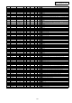
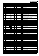
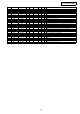
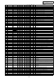
34 P62/RXD0 ZIMO I - - - Ed Z MAIN-ZONEμcom comm. control pIn
35 P61/CLK0 CLKZIMO I - - - Ed Z MAIN-ZONEμcom comm. control pIn
36 P60/CTS0/RTS0 REQZOMI O C - - Ed Z MAIN-ZONEμcom comm. control pIn
37 P57 NC O C - - - Z Not used
38 P56 NC O C - - - Z Not used
39 P55/EPM FRASH EPM I - Lv - Eu Z RewrIte boot start: L
40 P54 DIRCLK8Z O C - - - Z DIR8 control pIn (LC89057W-E), control clock output ( ※ used as DIR for ZONE2)
41 P53 DIR CE8Z O C - - - Z DIR8 control pIn (LC89057W-E), chIp enable output ( ※ used as DIR for ZONE2)
42 P52 DIR_RST8Z O C - - Ed Z DIR control output (LC89057W-E) Reset: L ( ※ used as DIR for ZONE2)
43 P51 DIRDIN8Z O C - - Eu Z DIR8 control pIn (LC89057W-E), control data output ( ※ used as DIR for
ZONE2)
44 P50/CE FRASH CE I - - - Ed Z RewrIte boot program start: H Input set
45 P47 DIRDOUT8 I - - - Eu Z DIR8 control Input pIn (LC89057W-E), control data Input ( ※ "Z"set: Operated
from SUBμcom)
46 P46 NC I - - - - Z Not used
47 P45 NC O C - - - Z Not used
48 P44 NC O C - - - Z Not used
49 P43 NC O C - - - Z Not used
50 P42 NC O C - - - Z Not used
51 P41 DAPLDSTBZ O C - - - Z FPGA control for DAC
52 P40 DAPLDCLKZ O C - - - Z FPGA control for DAC
53 P37 DAPLDDATAZ O C - - - Z FPGA control for DAC
54 P36 DAMSZ O C - - - Z FPGA control for DAC
55 P35 DAMDIZ O C - - - Z FPGA control for DAC
56 P34 DAMCZ O C - - - Z FPGA control for DAC
57 P33 NC O C - - - Z Not used
58 P32 NC O C - - - Z Not used
59 P31 NC O C - - - Z Not used
60 VCC VCC - - - - - - +5V
61 P30 NC O C - - - Z Not used
62 VSS VSS - - - - - - GND
63 P27 NC O C - - - Z Not used
64 P26 NC O C - - - Z Not used
65 P25 NC O C - - - Z Not used
66 P24 NC O C - - - Z Not used
67 P23 NC O C - - - Z Not used
68 P22 NC O C - - - Z Not used
69 P21 NC O C - - - Z Not used
70 P20 NC O C - - - Z Not used
71 P17/INT5 NC I - - - - Z Not used
72 P16/INT4 INT6 I - E ↓ &L - - Z DIR6 control pIn (LC89057W-E) ( ※ "Z"set: Operated from SUBμcom)
73 P15/INT3 INT7 I - E ↓ &L - - Z DIR7 control pIn (LC89057W-E) ( ※ "Z"set: Operated from SUBμcom)
74 P14/D12 MUTEZ2 O C - - - Z Mute control for DAC output ( ※ "Z"set: Operated from SUBμcom)
75 P13/D11 NC I - - - - Z Not used
76 P12/D10 NC I - - - - Z Not used
77 P11/D9 NC I - - - - Z Not used
78 P10/D8 STBZOPLDI O C - - - Z MAIN FPGA control pIn
79 P07/D7 CLKZOPLDI O C - - - Z MAIN FPGA control pIn
80 P06/D6 ZIPLDO I - - - - Z MAIN FPGA control pIn
81 P05/D5 ZOPLDI O C - - - Z MAIN FPGA control pIn
82 P04/D4 MUTEZ4 O C - - - Z Mute control for DAC output ( ※ "Z"set: Operated from SUBμcom)
83 P03/D3 MUTEZ3 O C - - - Z Mute control for DAC output ( ※ "Z"set: Operated from SUBμcom)
84 P02/D2 VPPZ I - - - - Z Normal: H WrItIng flash ROM for DSP: L
85 P01/D1 DSPA0Z O - - - - Z PLD control for DSP (3-bIt address for target selectIon of RST/CS)
86 P00/D0 DSPA1Z O - - - - Z PLD control for DSP (3-bIt address for target selectIon of RST/CS)
87 P107/AN7 DSPA2Z O - - - - Z PLD control for DSP (3-bIt address for target selectIon of RST/CS)
88 P106/AN6 NC O - - - - Z Not used
89 P105/AN5 DSPIOPOWERZ O C - - - Z DSP POWER ON="L" (After 10ms from DIGITAL POWER ON)
90 P104/AN4 NC O C - - - Z Not used
91 P103/AN3 DSPROMRSTZ O C - - - Z Not used
92 P102/AN2 DSPRSTZ O C - - - Z PLD control for DSP reset(Reset: L)
93 P101/AN1 DSPOSCONZ O C - - - Z ON="H"(After 20ms from DIGITAL POWER ON)
94 AVSS AVSS - - - - - - AD GND
95 P100/AN0 DSPBOOT I - - - Eu Z DSP rewrIte boot program (DSP rewrIte: L Input)
96 VREF VREF - - - - - - AD ref. +5V
97 AVCC AVCC - - - - - - AD +5V
98 P97/SIN4 DSPOZI I - - - - Z PLD control pIn for DSP
99 P96/SOUT4 DSPIZO O C - - - Z PLD control pIn for DSP
100 P95/CLK4 DSPCLKZ O C - - - Z PLD control pIn for DSP
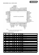
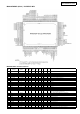
PIn PIn Name Symbol I/O Type Det
Op
(Int.)
Op
(Ext.)
Res FUNCTION