
User Guide

46
AVR-5805/AVC-A1XV
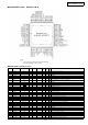
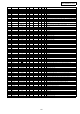
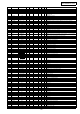
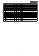
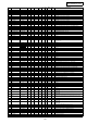
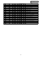
28 P77 DIRCLK1 O C - - - Z DIR1 control pin (LC89057W-E), control clock output
29 P76 DIRCE1 O C - - - Z DIR1 control pin (LC89057W-E), chip enable output
30 P75 ACKSIIEO I - - - Ed Z ETHERNET control pin
31 P74 RSTIE O C - - Eu Z ETHERNET reset output, Reset=”L”(Reset release="H" after 80msec from
IEPOWER ON)
32 P73/CTS2 CSIE O C - - Eu Z ETHERNET control pin
33 P72/CLK2 CLKSOIEI O C - - Eu Z ETHERNET control pin
34 P71/RXD2 SIIEO I N - - Eu Z ETHERNET control pin
35 P70/TXD2 SOIEI O N - - Eu Z ETHERNET control pin
36 P67/TXD1 TXD.S/(ZISO) O C - - - Z Data transfer output to outside /(ZONE-SUB μcom comm. control pin)
37 VCC1 VCC1 - - - - - Z +3.3V
38 P66/RXD1 RXD.S/(ZOSI) I - - - - Z Data receive input from outside /(ZONE-SUB μcom comm. control pin)
39 VSS VSS - - - - - Z GND
40 P65/CLK1 NC I - - - Ed Z Not used
41 P64/CTS1 NC O C - - Ed Z Not used
42 P63/TXD0 SOMI O C - - - Z MAIN-SUB μcom comm. control pin
43 P62/RXD0 SIMO I - - - - Z MAIN-SUB μcom comm. control pin
44 P61/CLK0 CLKSIMO I - - - - Z MAIN-SUB μcom comm. control pin
45 P60/CTS0 REQSOMI O C - - - Z MAIN-SUB μcom comm. control pin
46 P137 DIRDOUT8 I - - - Eu Z DIR8 control input pin (LC89057W-E), control data input ( ※ "Z"set: operated
from ZONE μcom)
47 P136 DIRCE5 O C - - - Z DIR5 control pin (LC89057W-E), chip enable output
48 P135 SUBnCE O C - - - Z FPGA rewrite control pin
49 P134 SUBTDI O - - - - Z PLD rewrite control pin(JTAG)
50 P57 SUBTMS O - - - - Z PLD rewrite control pin(JTAG)
51 P56 SUBTDO I - - - - Z PLD rewrite control pin(JTAG)
52 P55/EPM FRASH EPM I - Lv - Eu Z Rewrite boot program start: L
53 P54 SUBTCK O C - - - Z PLD rewrite control pin(JTAG)
54 P133 SUBDATAOUT I - - - - Z FPGA rewrite control pin
55 P132 SUBASDI O C - - - Z FPGA rewrite control pin
56 P131 SUBnCS O C - - - Z FPGA rewrite control pin
57 P130 SUBnCONFIG O C - - - Z FPGA rewrite control pin
58 P53 SUBDCLK O C - - - Z FPGA rewrite control pin
59 P52 SUBCONF_DONE I - - - - Z FPGA rewrite control pin
60 P51 SUBCPUJTAGON O C - - - Z JTAG (PLD rewrite from SUB-μcom:L) ※ default → D.POWER OFF: H
61 P50/CE FRASH CE I - - - Ed Z Rewrite boot program start: H
62 P127 FRONTJTAGON O C - - - Z JTAG (PLD rewrite from FRONT:L) ※ default → D.POWER OFF: H
63 P126 FRONTASON O C - - - Z Active Serial on(FPGA rewrite from FRONT:L) ※ default → D.POWER OFF: H
64 P125 SUBCPUASON O C - - - Z Active Serial on(FPGA rewrite from SUB-μCOM:L) ※ default → D.POWER OFF:
H
65 P47 DSPJTAGON O C - - - Z Fixed to L
66 P46 NC O C - - - Z Not used
67 P45 OSCON O C - - - Z Oscillator for DIR CLK(Osc. Stop:L)
68 P44 NC O C - - - Z Not used
69 P43 NC O C - - - Z Not used
70 P42 NC O C - - - Z Not used
71 P41 DIRRST1 O C - - - Z DIR1 ∼ 5 control output (LC89057W-E) Reset: L
72 P40 DPOWER O C - - Ed Z DIGITAL power on/off switching(ON:H)
73 P37 IEPOWER O C - - Ed Z ETHERNET power control(ON:H)
74 P36 RSV1394 O C - - - Z 1394 control pin
75 P35 MOSI1394PLD O C - - - Z 1394 control pin
76 P34 CLK1394PLD O C - - - Z 1394 control pin
77 P33 CS1394PLD O C - - - Z 1394 control pin
78 P32 DINPLDREQ I - - - - Z PLD control for DIGITAL INPUT
79 P31 DINPLDOSI I - - - - Z PLD control for DIGITAL INPUT
80 P124 DINPLDISO O C - - - Z PLD control for DIGITAL INPUT
81 P123 DINPLDCS O C - - - Z PLD control for DIGITAL INPUT
82 P122 DINPLDCLK O C - - - Z PLD control for DIGITAL INPUT
83 P121 NC O C - - - Z Not used
84 P120 NC O C - - - Z Not used
85 VCC2 VCC2 - - - - - - +3.3V
86 P30 NC O C - - - Z Not used
87 VSS VSS - - - - - - GND
88 P27 NC O C - - - Z Not used
89 P26 NC I - - - Eu Z Not used
90 P25 NC I - - - Eu Z Not used
91 P24 NC I - - - Eu Z Not used
92 P23 NC I - - - Eu Z Not used
93 P22 NC I - - - Eu Z Not used
94 P21 NC I - - - Eu Z Not used
95 P20 MUTE1 O C - - - Z Mute control for DAC output
96 P17/INT5 1394+12VON O C - - Eu Z 1394 +12V ON:H (TPS67341) ※ same logic as IEPOWER
97 P16/INT4 INT1
I - E ↓ &L - Eu Z DIR1 control pin (LC89057W-E)
98 P15/INT3 NC I - - - - Z Not used
99 P14 NC I - - - Eu Z Not used
100 P13 NC I - - - Eu Z Not used
101 P12 DAMDIS O C - - - Z FPGA control for DAC
102 P11 DAMCS O C - - - Z FPGA control for DAC
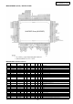
Pin Pin Name Symbol I/O Type Det
Op
(Int.)
Op
(Ext.)
Res FUNCTION