
User Guide

55
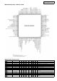
AVR-5805/AVC-A1XV
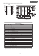
BR24L02F-WE2 (IC101,102,201,202) D,VIDEO P.W.B.
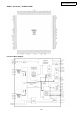
SN65LVDS1DBVR (IC102) AD P.W.B.
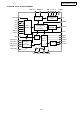
SN65LVDS1DBVR (IC108) D.VIDEO P.W.B.
SN65LVDS1DBVR (IC402) DIGITAL P.W.B
Block diagram
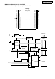
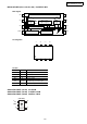
1
A0
A1 2
A2 3
GND 4
V
CC
8
WP7
6 SCL
SDA5
2kbit EEPROM array
Control logic
High voltage generator Vcc level detect
8bit
8bit
ACK
STOPSTART
Address
decoder
Slave word
address register
8bits
Data
register
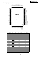
Pin configuration
V
CC
A0
WP
A1
SCL
A2
SDA
GND
1234
5678
Pin name
Write protect input
Power supply
Function
Ground (0V)
Slave address set
Serial clock input
SDA
V
CC
A0, A1, A2
Pin name
GND
WP
SCL
I / O
IN
IN
IN
IN / OUT
Slave and word address,
serial data input, serial data output
1 An open drain output requires a pull-up resistor.
1
3
2
4
5
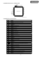
(TOP VIEW)
1
V
CC
GND
Z
D
Y