
User Guide

59
AVR-5805/AVC-A1XV
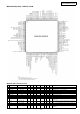
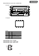
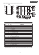
PCM1792DBR (IC201-204,401,402,501,502) DAC P.W.B.
1
2
3
4
5
6
7
8
9
10
11
12
13
14
28
27
26
25
24
23
22
21
20
19
18
17
16
15
ZEROL
ZEROR
MSEL
LRCK
DATA
BCK
SCK
DGND
V
DD
MS
MDI
MC
MDO
RST
V
CC
2L
AGND3L
I
OUT
L−
I
OUT
L+
AGND2
V
CC
1
V
COM
L
V
COM
R
I
REF
AGND1
I
OUT
R−
I
OUT
R+
AGND3R
V
CC
2R
(TOP VIEW)
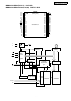
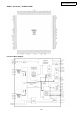
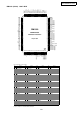
FUNCTIONAL BLOCK DIAGRAM
Power Supply
RST
SCK
Advanced
Segment
DAC
Modulator
I
OUT
L+
I
OUT
L−
I
OUT
R−
Current
Segment
DAC
I
OUT
R+
Bias
and
Vref
V
COM
L
V
COM
R
AGND2
V
DD
V
CC
1
V
CC
2L
V
CC
2R
AGND1
I/V and Filter
8
Oversampling
Digital
Filter
and
Function
Control
Audio
Data Input
I/F
LRCK
BCK
DATA
MDO
MDI
MC
MS
AGND3L
AGND3R
DGND
Current
Segment
DAC
I
REF
V
OUT
L
I/V and Filter
V
OUT
R
Function
Control
I/F
MSEL
Zero
Detect
ZEROL
ZEROR
System
Clock
Manager
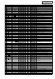
Terminal Functions
TERMINAL
I/O
DESCRIPTIONS
NAME PIN
I/O
DESCRIPTIONS
AGND1 19 − Analog ground (internal bias)
AGND2 24 − Analog ground (internal bias)
AGND3L 27 − Analog ground (L-channel DACFF)
AGND3R 16 − Analog ground (R-channel DACFF)
BCK 6 I Bit clock input
(1)
DATA 5 I Serial audio data input for normal operation
(1)
DGND 8 − Digital ground
I
OUT
L+ 25 O L-channel analog current output+
I
OUT
L– 26 O L-channel analog current output–
I
OUT
R+ 17 O R-channel analog current output+
I
OUT
R– 18 O R-channel analog current output–
I
REF
20 − Output current reference bias pin
LRCK 4 I Left and right clock (f
S
) input for normal operation
(1)
MC 12 I Mode control clock input
(1)
MDI 11 I Mode control data input
(1)
MDO 13 I/O Mode control readback data output
(3)
MS 10 I/O Mode control chip-select input
(2)
MSEL 3 I I
2
C/SPI select
(1)
RST 14 I Reset
(1)
SCK 7 I System clock input
(1)
V
CC
1 23 − Analog power supply, 5 V
V
CC
2L 28 − Analog power supply (L-channel DACFF), 5 V
V
CC
2R 15 − Analog power supply (R-channel DACFF), 5 V
V
COM
L 22 − L-channel internal bias decoupling pin
V
COM
R 21 − R-channel internal bias decoupling pin
V
DD
9 − Digital power supply, 3.3 V
ZEROL 1 I/O Zero flag for L-channel
(2)
ZEROR 2 I/O Zero flag for R-channel
(2)
(1)
Schmitt-trigger input, 5-V tolerant
(2)
Schmitt-trigger input and output. 5-V tolerant input and CMOS output
(3)
Schmitt-trigger input and output. 5-V tolerant input. In I
2
C mode, this pin becomes an open-drain 3-state output; otherwise, this pin is a CMOS
output.