
User Guide

63
AVR-5805/AVC-A1XV
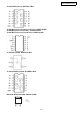
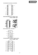
TC9274F-022 (IC120,213,214,401,402) AUDIO P.W.B.
TPS6734IDR (IC301) DIGITAL P.W.B.
1
2
3
4
8
7
6
5
EN
REF
SS
COMP
V
CC
FB
OUT
GND
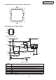
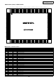
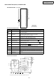
functional block diagram
EN
1
EN
7
EN
FB
_
+
4
COMP
Voltage
Reference
x3.5
SS
Clamp
Error
Amplifier
PWM
Comparator
R
S
170-kHz
Oscillator
V
CC
Power Switch
Drive Latch
Σ
2
REF
3
SS
x6
Current
Sense Amplifier
Overcurrent
Comparator
Driver
V
CC
OUT
GND
8
6
5
+
1 MΩ
–
Q
Terminal Functions
TERMINAL
DESCRIPTION
NAME NO.
DESCRIPTION
EN 1 Enable. EN ≥ 2 V turns on the TPS6734. EN ≤ 0.4 V turns it off and reduces the supply current to 3 µA max.
REF 2 1.22-V reference voltage output. REF can source 100 µA for external loads.
SS 3 Soft Start. A capacitor between SS and GND brings the output voltage up slowly at power-up.
COMP 4 Compensation connection. A 0.001-µF capacitor between COMP and FB stabilizes the feedback loop.
GND 5 Ground
OUT 6 N-channel MOSFET drain connection
FB 7 Feedback voltage. FB is connected to the converter output for the feedback loop.
V
CC
8 Supply voltage input