
User Guide

70
AVR-5805/AVC-A1XV
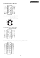
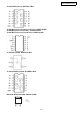
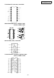
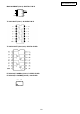
K4S161622H-TC60 (IC413) D.VIDEO P.W.B.
VDD
DQ0
DQ1
V
SSQ
DQ2
DQ3
V
DDQ
DQ4
DQ5
V
SSQ
DQ6
DQ7
V
DDQ
LDQM
WE
CAS
RAS
CS
BA
A10/AP
A0
A1
A2
A3
V
DD
1
2
3
4
5
6
7
8
9
10
11
12
13
14
15
16
17
18
19
20
21
22
23
24
25
50
49
48
47
46
45
44
43
42
41
40
39
38
37
36
35
34
33
32
31
30
29
28
27
26
PIN CONFIGURATION (TOP VIEW)
VSS
DQ15
DQ14
V
SSQ
DQ13
DQ12
V
DDQ
DQ11
DQ10
V
SSQ
DQ9
DQ8
V
DDQ
N.C/RFU
UDQM
CLK
CKE
N.C
A9
A8
A7
A6
A5
A4
V
SS
50PIN TSOP (II)
(400mil x 825mil)
(0.8 mm PIN PITCH)
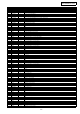
PIN FUNCTION DESCRIPTION
Pin Name Input Function
CLK System Clock Active on the positive going edge to sample all inputs.
CS
Chip Select
Disables or enables device operation by masking or enabling all inputs except
CLK, CKE and L(U)DQM
CKE Clock Enable
Masks system clock to freeze operation from the next clock cycle.
CKE should be enabled at least one cycle prior to new command.
Disable input buffers for power down in standby.
A
0 ~A10/AP Address
Row / column addresses are multiplexed on the same pins.
Row address : RA
0 ~RA10, column address : CA0 ~CA7
BA Bank Select Address
Selects bank to be activated during row address latch time.
Selects bank for read/write during column address latch time.
RAS
Row Address Strobe
Latches row addresses on the positive going edge of the CLK with RAS
low.
Enables row access & precharge.
CAS
Column Address Strobe
Latches column addresses on the positive going edge of the CLK with CAS
low.
Enables column access.
WE
Write Enable
Enables write operation and row precharge.
Latches data in starting from CAS
,WEactive.
L(U)DQM Data Input/Output Mask
Makes data output Hi-Z, t
SHZ after the clock and masks the output.
Blocks data input when L(U)DQM active.
DQ
0 ~ 15 Data Input/Output Data inputs/outputs are multiplexed on the same pins.
V
DD/VSS Power Supply/Ground Power and ground for the input buffers and the core logic.
V
DDQ/VSSQ Data Output Power/Ground
Isolated power supply and ground for the output buffers to provide improved noise
immunity.
N.C/RFU
No Connection/
Reserved for Future Use
This pin is recommended to be left No Connection on the device.
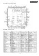
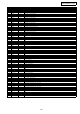
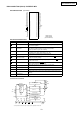
FUNCTIONAL BLOCK DIAGRAM
* Samsung Electronics reserves the right to change products or specification without notice.
Bank Select
Data Input Register
512Kx16
512Kx16
Sense AMP
Output BufferI/O Control
Column Decoder
Latency & Burst Length
Programming Register
Address Register
Row Buffer
Refresh Counter
Row Decoder Col. Buffer
LRAS
LCBR
LCKE
LRAS LCBR LWE LDQM
CLK CKE CS
RAS CAS WE L(U)DQM
LWE
LDQM
DQi
CLK
ADD
LCAS LWCBR
Timing Register