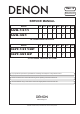
e Ver. 3 Please refer to the MODIFICATION NOTICE. SERVICE MANUAL MODEL JP E3 E3B AVR-1311 E2 EK EA E1 3 AVR-391 E1C 3 3 3 AV SURROUND RECEIVER MODEL JP E3 E3B DHT-1311XP DHT-391XP E2 EK 3 3 3s 5.1CH HOME THEATER SYSTEM • For purposes of improvement, specifications and design are subject to change without notice. • Please use this service manual with referring to the operating instructions without fail.
SAFETY PRECAUTIONS The following check should be performed for the continued protection of the customer and service technician. LEAKAGE CURRENT CHECK Before returning the unit to the customer, make sure you make either (1) a leakage current check or (2) a line to chassis resistance check. if the leakage current exceeds 0.5 milliamps, or if the resistance from chassis to either side of the power cord is less than 460 kohms, the unit is defective.
NOTE FOR SCHEMATIC DIAGRAM WARNING: Parts marked with this symbol z have critical characteristics. Use ONLY replacement parts recommended by the manufacturer. CAUTION: Before returning the unit to the customer, make sure you make either (1) a leakage current check or (2) a line to chassis resistance check. If the leakage current exceeds 0.5 milliamps, or if the resistance from chassis to either side of the power cord is less than 460 kohms, the unit is defective.
SYSTEM CONFIGURATION • AVR-1311 • AVR-391 • DHT-1311XP (AVR-1311 + SYS-391HT) • DHT-391XP (AVR-391 + SYS-391HT) SYS-391HT : Refer to page 104-113 for the service manual. SYS-391HT DSW-391 SC-F391(x2) SC-R391(x2) SC-C391 TECHNICAL SPECIFICATIONS n Audio Section n Tuner section [FM](Note: μV at 75 Ω, 0 dBf = 1 x 10–15 W) s Receiving Range (for 391E3,391E3B) : [AM]520 kHz – 1710 kHz [FM] 87.5 MHz – 107.9 MHz Receiving Range (for 1311E2,1311E1C,391EA) : [AM]522 kHz – 1611 kHz [FM] 87.5 MHz – 108.
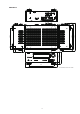
146.5 30.5 166.5 86.0 20.0 30.0 340.0 435.0 The illustration is AVR-1311 model. 5 381.4 338.5 20.7 43.5 43.5 248.0 245.0 22.
CAUTION IN SERVICING Initializing AV SURROUND RECEIVER AV SURROUND RECEIVER initialization should be performed when the μcom, peripheral parts of μcom, and Digital P.W.B. are replaced. 1. Turn off the power using ON/STANDBY button. 2. Press ON/STANDBY button while simultaneously pressing SURROUND MODE 0 and SURROUND MODE 1 buttons. 3. Check that the entire display is flashing with an interval of about 1 second, and release your fingers from the 2 buttons and the microprocessor will be initialized.
DISASSEMBLY • Disassemble in order of the arrow of the figure of following flow. • In the case of the re-assembling, assemble it in order of the reverse of the following flow. • In the case of the re-assembling, observe "attention of assembling" it. • If wire bundles are untied or moved to perform adjustment or parts replacement etc., be sure to rearrange them neatly as they were originally bundled or placed afterward. Otherwise, incorrect arrangement can be a cause of noise generation.
1. FRONT PANEL ASSY Proceeding : TOP COVER → FRONT PANEL ASSY (1) Remove the screws. View from bottom (2) Cut the wire clamp band, then disconnect the connector wires and FFC cable. Remove the screws. FFC cable FRONT PANEL ASSY CN44 CN71 cut cut CN209 WIRE SUPPORT UNIT (3) Remove the screws. Please refer to "EXPLODED VIEW" for the disassembly method of each P.W.B included in FRONT PANEL ASSY.
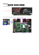
2. HDMI UNIT Proceeding : TOP COVER → HDMI UNIT (1) Remove the screws. Direction of photograph: A (2) Disconnect the connector wire and FFC cable.
3. INPUT UNIT Proceeding : TOP COVER → HDMI UNIT → INPUT UNIT (1) Remove the screws. Direction of photograph: A (2) Disconnect the connector wires and FFC cables, then remove the screws.
4. RADIATOR ASSY Proceeding : TOP COVER → HDMI UNIT → INPUT UNIT RADIATOR ASSY → (1) Remove the screws. Direction of photograph: A (2) Disconnect the connector wires, then remove the screws.
(3) Remove the RADIATOR ASSY from the main unit. Direction of photograph: C Please refer to "EXPLODED VIEW" for the disassembly method of each P.W.B included in RADIATOR ASSY. 5. POWER UNIT Proceeding : TOP COVER → POWER UNIT Please refer to "EXPLODED VIEW" for the disassembly method of POWER UNIT. 6. POWER TRANS Proceeding : CABINET TOP → TRANS MAIN Please refer to "EXPLODED VIEW" for the disassembly method of POWER TRANS.
SPECIAL MODE Special mode setting button b Press the ON/STANDBY button to turn on while pressing both buttons A and B at the same time. Mode Button A Button B STATUS DIMMER Initialization mode SURROUND MODE 0 SURROUND MODE 1 Backup data initialization is carried out. (Refer to page 6.) Mode for switching tuner frequency step SURROUND MODE 0 RESTORER ---E2 model only--Change tuner frequency step to AM9k/FM50kHz STEP or AM:10k/FM:200kHz.
1. μcom/DSP Version display mode 1.1. Operation specifications μcom/DSP version display mode: When started up, the version information is displayed. Starting up: With the "DIMMER" and "STATUS" buttons pressed, press the "ON/STANDBY" button to turn the power on. Now, press the "STATUS" button to the display the 2nd item information on the FL Display. 1.2.
ABOUT REPLACE THE MICROPROCESSOR WITH A NEW ONE When replaced of the U-PRO (Microprocessor) or the Flash ROM, confirm contents of the following. PWB Name Ref. No. After replaced Description Remark DIGITAL IC91 T5CN5 B SOFTWARE: Main DIGITAL IC82 ST25VF080B-50-4C-S2AF B SOFTWARE: DSP ROM After replaced A : Mask ROM (With software). No need write-in of software to the microprocessor. B : Flash ROM (With software). Usually, no need write-in of software.
2. UPDATE FIRMWARE (1) Connect the update terminal of AV receiver with the “Writing Kit”. (2) Set the switch of “Writing Kit" (Refer to the table below). DSPBOOT H CE H EPM H CNVSS H (3) Press the "ON/STANDBY" button to turn the power on of AV receiver. (4) Set the switch of “Writing Kit" (Refer to the table below). DSPBOOT H CE H EPM L CNVSS H (5) Press the "RESET" switch of “Writing Kit". (6) Run the “BootTool_M330(Writing program).exe” on desktop of PC. (7) Click the “Connect” button.
DSP SF1 (8) Choose Ram File(OnBoard_M330.s32). Choose Ram File(OnBoard_M330.s32).
(9) Choose Flash File(DSP : SF1). Choose "AVR1311_SF1_*_*_*_01.s32". Choose "Hex File (*.S32)".
(10) Click the “Start” button. The Setup Status bar appears.
(11) "Finished!!" is displayed. Click the "OK"” button. (12) Set the switch of “Writing Kit" (Refer to the table below). DSPBOOT H CE H EPM H CNVSS H (13) Press the "RESET" switch of “Writing Kit". (14) AV receiver is power on and starts update of DSP1. (15) "Write Comleted" is displayed in the FL tube. (16) Set the switch of “Writing Kit" (Refer to the table below). DSPBOOT H CE H EPM L CNVSS H (17) Press the "RESET" switch of “Writing Kit". DSP SF2 (18) Click the “Resend” button.
(19) Choose Flash File(DSP : SF2). Choose "AVR1311_SF2_*_*_*_01.s32". Choose "Hex File (*.S32)".
(20) Click the “Start” button. The Setup Status bar appears. (21) "Finished!!" is displayed. Click the "OK"” button.
(22) Set the switch of “Writing Kit" (Refer to the table below). DSPBOOT H CE H EPM H CNVSS H (23) Press the "RESET" switch of “Writing Kit". (24) AV receiver is power on and starts update of DSP2. (25) "Write Comleted" is displayed in the FL tube. (26) Set the switch of “Writing Kit" (Refer to the table below). DSPBOOT H CE H EPM L CNVSS H (27) Press the "RESET" switch of “Writing Kit". MAIN (28) Click the “Resend” button. "Connected" is displayed, it is OK.
(29) Choose Flash File(MAIN). Choose "AVR1311.s32". Choose "Hex File (*.S32)".
(30) Click the “Start” button. The Setup Status bar appears. (31) "Finished!!" is displayed. Click the "OK"” button.
(32) Set the switch of “Writing Kit" (Refer to the table below). DSPBOOT H CE H EPM H CNVSS H (33) Press the "RESET" switch of “Writing Kit". (34) Initializing. 1. Turn off the power using ON/STANDBY button. 2. Press ON/STANDBY button while simultaneously pressing SURROUND MODE 0 and SURROUND MODE 1 buttons. 3. Check that the entire display is flashing with an interval of about 1 second, and release your fingers from the 2 buttons and the microprocessor will be initialized.
ADJUSTMENT Audio Section Idling Current Required measurement equipment: DC Voltmeter 1. Preparation (1) Avoid direct blow from an air conditioner or an electric fan, and adjust the unit at normal room temperature 15 °C ~ 30 °C. (2) Presetting • POWER (Power source switch) OFF • SPEAKER (Speaker terminal) No load (Do not connect speaker, dummy resistor, etc.) 2. Adjustment (1) emoved top cover and set VR41(FL),VR45(FR),VR42(C),VR44(SL),VR43(SR), on Main Amp. Unit at fully counterclockwise position.
Symbols in the table D D D D D D D D D S S S S S S S S S S S DOLBY PRO LOGIC g DTS NEO:6 DOLBY DIGITAL DOLBY DIGITAL Plus DOLBY TrueHD DTS SURROUND DTS 96/24 DTS-HD DTS Express MULTI CH STEREO VIRTUAL z1 z2 z3 z4 z5 D S D D D D D D D D D D D D D D D D D D D D D A signal for each channel contained in an input signal is output as audio. Only when “Mode” is set to “LFE+Main”, sound is output from the subwoofer.
z2 z6 z7 S S S S S S S S S S DTS 96/24 DTS-HD DTS Express VIRTUAL Only when “Mode” is set to “LFE+Main”, sound is output from the subwoofer. This item can be selected when a Dolby Digital or DTS or DVD-Audio signal is played. This item can be set when the input signal is analog, PCM 48 kHz or 44.1 kHz.
Symbols in the table DTS SURROUND DTS-HD MSTR DTS-HD HI RES DTS ES DSCRT6.1 DTS ES MTRX6.
MULTI CH IN MULTI CH IN MULTI CH IN + PLgx CINEMA MULTI CH IN + PLgx MUSIC MULTI CH IN 7.1 DIRECT DIRECT DSP SIMULATION MULTI CH STEREO VIRTUAL STEREO STEREO Surround mode S S S S S S F F S S F D (7.1) F S S S LINEAR PCM LINEAR PCM (multi ch) (2ch) S ANALOG S S DTS-HD Master Audio S S DTS-HD High Resolution Audio DTS-HD S S DTS EXPRESS S S S S DTS ES DSCRT (With Flag) S S S S S S S S DTS (5.
TROUBLE SHOOTING 1. POWER 1.1. Power not turn on Power not turn on. Is the ON/STANDBY indicator on the front panel flashing red? YES Are there any incomplete connections in the connectors connecting between the various circuit boards? NO YES YES Correct the short circuit between the speaker and ground. NO Check for damage in the power amplifier circuitry parts and replace any defective parts. Connect the connectors property.
2. Analog video MONITOR OUT(CVBS) Output NG Check ±5V +5V : C755 -5V : C754 NG The power supply circuitry is defective. OK NG Check output Output V : IC71-1pin The IC71 and surrounding circuitry is defective. OK Check cable between main unit and monitor or Check monitor. AVR-1311 model only MONITOR OUT(COMPONENT) Output NG NG Check ±5V +5V : C797 -5V : C799 The power supply circuitry is defective. OK NG The IC73 and surrounding circuitry is defective.
3. HDMI/DVI 3.1. No picture or sound is output No picture or sound is output. Check HDMI/DVI cable connection. NO (1) Is the HDMI/DVI cable properly connected? There may be a problem with the HDMI/DVI cable. Check connection.
Check TV NO (10) Is the TV HDCP-compatible? Use an HDCP-compatible TV. PC TVs cannot be used. YES NO (11) Is the TV compatible with resolutions of 1080P? If the TV is not compatible with resolutions of 1080P, no picture will be output, even if the BD/DVD player's resolution is set to 1080P. YES NO (12) Is the TV's input set to HDMI? Check TV's input setting, referring to the TV's operating instructions. YES NO (13) Are the picture and sound output when a different TV is used? The TV is defective.
NO (19) Check xtal oscillator. Is there 28.6363MHz oscillation of X101? The X101 or IC11 is defective. YES (20) Check RESET. Is RESET waveform confirmed in IC11 (97pin), when power is turned on? (If continued to "H" or " L", proceed to "NO".) NO The RESET pattern or IC11 is defective. YES (21) Check control signal(I2C). Is waveform confirmed in IC11 78pin(SDATA)/79pin(SCL). (If not continued to " L", proceed to "YES".) YES HDMI output circuitry is defective (IC11 and surrounding circuitry).
3.2.
DDC_CLK/DDC_DATA/TMDS : Check item (15),(17) 0.9V DDC_CLK TMDS SIGNAL 2.
㪩㪤㪚㪢㩿㪌㪌㪀 CH2: fs CH3: 64fs CH4: 256fs 㽴 㩿㪈㪍㪀㪯㪫㪘㪣㪶㪦㪬㪫 㩿㪊㪊㪀㪛㪘㪠㪉㪶㪪㪚㪣㪢 㩿㪌㪋㪀㪛㪘㪦㪈㪶㪣㪩㪚㪣㪢 㪪㪘㪠㪶㪪㪛㪦㪬㪫㩿㪌㪋㪀 㩿㪌㪉㪀㪛㪘㪦㪈㪶㪪㪚㪣㪢 㩿㪊㪉㪀㪛㪘㪠㪉㪶㪣㪩㪚㪢 㩿㪌㪈㪀㪛㪘㪦㪈㪶㪛㪘㪫㪘㪇㪃㪟㪪㪇 㪪㪘㪠㪶㪚㪣㪢㩿㪍㪈㪀 㪪㪘㪠㪶㪣㪩㪚㪢㩿㪍㪇㪀 㩿㪋㪐㪀㪛㪘㪦㪈㪶㪛㪘㪫㪘㪈㪃㪟㪪㪈 䇭 㪛㪘㪦㪶㪤㪚㪣㪢㩿㪋㪇㪀 㪛㪘㪠㪈㪶㪪㪚㪣㪢㪃㪛㪪㪛㪄㪚㪣㪢㩿㪉㪐㪀 㪛㪘㪠㪈㪶㪣㪩㪚㪢㪃㪛㪪㪛㪋㩿㪊㪇㪀 㪛㪘㪠㪈㪶㪛㪘㪫㪘㪊㪃㪛㪪㪛㪊㩿㪉㪊㪀 㪛㪘㪠㪈㪶㪛㪘㪫㪘㪉㪃㪛㪪㪛㪉㩿㪉㪋㪀 㩿㪐㪍㪀㪤㪚㪣㪢㪶㪦㪬㪫 㩿㪐㪌㪀㪪㪚㪣㪢㪶㪦㪬㪫 㩿㪐㪋㪀㪘㪧㪌㪶㪦㪬㪫 㩿㪐㪈㪀㪘㪧㪋㪶㪦㪬㪫 㩿㪐㪇㪀㪘㪧㪊㪶㪦㪬㪫 㩿㪏㪐㪀㪘㪧㪉㪶㪦㪬㪫 㩿㪏㪎㪀㪘㪧㪇㪶㪦㪬㪫 㩿㪏㪏㪀㪘㪧㪈㪶㪦㪬㪫 CH1: DATA 㪛㪘㪠㪈㪶㪛㪘㪫㪘㪈㪃㪛㪪㪛㪈㩿㪉㪍㪀 2 㪛㪘㪠㪈㪶㪛㪘㪫㪘㪇㪃㪛㪪㪛㪇㩿㪉㪎㪀 CH2: fs 㩿㪋㪏㪀㪛㪘㪦㪈㪶㪛㪉㪃㪟㪪㪉 㩿㪋㪐㪀㪩㪯㪧㪇 㩿㪋㪎㪀㪛㪘㪦㪈㪶
BLOCK DIAGRAM 40
LAEVEL DIAGRAM 44
PRINTED WIRING BOARDS FRONT (COMPONENT SIDE) d 1 2 3 4 5 6 7 8 9 10 11 12 13 14 15 16 17 18 A B C D E F G HEADPHONE (COMPONENT SIDE) d PHONE (COMPONENT SIDE) d 1 2 3 4 5 1 2 REGULATOT (COMPONENT SIDE) d 3 1 2 3 4 5 6 7 A A A B B B C C C D D 鉛フリー半田 半田付けには、鉛フリー半田 (Sn-Ag-Cu) を使用してください。 Lead-free Solder When soldering, use the Lead-free Solder (Sn-Ag-Cu).
FRONT (FOIL SIDE) d 18 17 16 15 14 13 12 11 10 9 8 7 6 5 4 3 2 1 A B C D E F G HEADPHONE (FOIL SIDE) d PHONE (FOIL SIDE) d 5 4 3 2 1 3 2 REGULATOT (FOIL SIDE) d 1 7 6 5 4 3 2 1 A A A B B B C C C D D 鉛フリー半田 半田付けには、鉛フリー半田 (Sn-Ag-Cu) を使用してください。 Lead-free Solder When soldering, use the Lead-free Solder (Sn-Ag-Cu).
AUX (COMPONENT SIDE) d VOLUME (COMPONENT SIDE) d 1 2 3 4 1 2 POWER (COMPONENT SIDE) d 3 1 4 2 3 A A A B B B C C C D AUX (FOIL SIDE) d VOLUME (FOIL SIDE) d 4 3 D 2 1 4 POWER (FOIL SIDE) d 3 2 1 3 2 1 A A A B B B C C C D D 鉛フリー半田 半田付けには、鉛フリー半田 (Sn-Ag-Cu) を使用してください。 Lead-free Solder When soldering, use the Lead-free Solder (Sn-Ag-Cu).
MAIN (COMPONENT SIDE) d 1 2 3 4 5 6 7 8 9 10 11 12 13 14 15 16 17 A B C D E F G H I Bar code J 鉛フリー半田 半田付けには、鉛フリー 半田 (Sn-Ag-Cu) を使用 K L してください。 Lead-free Solder When soldering, use the Lead-free Solder (Sn-Ag-Cu).
INPUT (COMPONENT SIDE) d 1 2 3 4 5 6 7 8 9 10 11 12 13 14 15 16 17 A B C D E F G H I J K 鉛フリー半田 半田付けには、 鉛フリー半田 (Sn-Ag-Cu) を使 L 用してください。 Lead-free Solder When soldering, use the Leadfree Solder (Sn-Ag-Cu).
INPUT (FOIL SIDE) d 17 16 15 14 13 12 11 10 9 8 7 6 5 4 3 2 1 A B C D E F G H I J 鉛フリー半田 K 半田付けには、 鉛フリー半田 (Sn-Ag-Cu) を使 用してください。 L Lead-free Solder When soldering, use the Leadfree Solder (Sn-Ag-Cu).
HDMI (COMPONENT SIDE) 1 2 3 4 5 6 7 8 9 10 11 12 13 A B C D E F G 鉛フリー半田 半田付けには、鉛フリー半田 (Sn-Ag-Cu) を使用してください。 Lead-free Solder When soldering, use the Lead-free Solder (Sn-Ag-Cu).
HDMI (FOIL SIDE) 13 12 11 10 9 8 7 6 5 4 3 2 1 A B C D E F G 鉛フリー半田 半田付けには、鉛フリー半田 (Sn-Ag-Cu) を使用してください。 Lead-free Solder When soldering, use the Lead-free Solder (Sn-Ag-Cu).
1 2 3 4 5 6 7 8 A B C D E d F SCHEMATIC DIAGRAMS (1/7) 54
1 2 3 4 5 6 7 8 HDMI_MCLK HDMI_SCLK HDMI_LRCLK 18 19 HDMI_SDATA2 17 HDMI_SDATA1 15 14 13 12 10 9 8 7 6 5 4 3 2 1 +5VH NOT USED SO HOLD WP SCK GND SI OPEN OPEN R165 +3V3H 0.1uF C138 10uF/6.3V C139 0.1uF C140 10uF/6.
1 2 3 4 5 6 7 8 A B C D E ANALOG AUDIO SIGNAL LINE SCHEMATIC DIAGRAMS (3/7) 56 d F
1 2 3 4 5 6 7 8 A B C D E VIDEO SIGINAL LINE COMPONENT (Y) SIGNAL LINE dF SCHEMATIC DIAGRAMS (4/7) 57
1 2 3 4 5 6 7 8 A B C D E ANALOG AUDIO SIGNAL LINE DIGITAL AUDIO SIGINAL LINE SCHEMATIC DIAGRAMS (5/7) 58 d F
1 2 3 4 5 6 7 8 A B C D E dF SCHEMATIC DIAGRAMS (6/7) 59
1 2 3 4 5 6 7 8 A B C D E ANALOG AUDIO SIGNAL LINE SCHEMATIC DIAGRAMS (7/7) 60 d F
WIRING DIAGRAM 61
EXPLODED VIEW C16 S5 X2 M11 AVR1311 S10 X4 S7 M4 S12 X3 C14 C13 M11 X10 S7 X2 M12 S5 z X17 M11 M10 S8 S8 X3 M5 X2 C12 M11 M3 C11 AVR1311 S3 X2 M9 S3 P13 X2 S3 S9 S8 C7 S3 X2 X2 X4 C6 S3 X4 M8 S6 S8 X6 M7 S1 X17 C10 P10 P11 P4 P6 C8 M4 X3 C5 C9 S3 S4 X17 S3 S3 C15 AVR391 X2 M3 M1 S2 S4 C4 X2 S7 M6 P9 P7 S4 S8 P7 X2 S11 X5 P3 M1 P4 X2 S5 X17 M2 X2 X2 S4 S7 P8 P12 S2 X10 P5 P6 C1 C2 AVR391 P8 M5 C3 S8 X4 P2 WARNING: Par
PARTS LIST OF EXPLODED VIEW zParts for which "nsp" is indicated on this table cannot be supplied. zP.W.B. ASS'Y for which "nsp" is indicated on this table cannot be supplied. When repairing the P.W.B. ASS'Y, check the board parts table and order replacement parts. zPart indicated with the mark " ★ " is not illustrated in the exploded view. zThe parts listed below are for maintenance only, might differ from the parts used in the unit in appearances or dimensions.
Ref.No. Part No.
Ref.No. Part No.
PACKING VIEW (for AVR-1311, 391) 5-1 6 7 8 9 10 3 1 z 4 2 5-2 13 14 12 11 11 12 14 13 PARTS LIST OF PACKING & ACCESSORIES (for AVR-1311, 391) zParts for which "nsp" is indicated on this table cannot be supplied. zPart indicated with the mark " ★ " is not illustrated in the exploded view. zThe parts listed below are for maintenance only, might differ from the parts used in the unit in appearances or dimensions. Note: The symbols in the column "Remarks" indicate the following destinations.
Ref.No. Part No. Part Name Remarks 8 00D9430113403 FM 1 POLE ANT.
PACKING VIEW (for DHT-1311XP, 391XP) 5-1 6 7 8 9 10 3 1 z 4 2 11 5-2 SYS-391HT 14 (Refer to page 109,110.) 13 13 12 PARTS LIST OF PACKING & ACCESSORIES (for DHT-1311XP, 391XP) zParts for which "nsp" is indicated on this table cannot be supplied. zPart indicated with the mark " ★ " is not illustrated in the exploded view. zThe parts listed below are for maintenance only, might differ from the parts used in the unit in appearances or dimensions.
Ref.No. 4 Part No. Part Name Remarks 943533009940D SNOW PAD(R) CPS1A883 Q'ty New 1 * 5-1 541110486002D INSTRUCTION MANUAL A 1311SPE2,1311BKE2 CQX1A1538Z 1 * 5-2 541110603005D INSTRUCTION MANUAL B 1311SPE2,1311BKE2 CQX1A1538Y 1 * 5-1 541110484006D INSTRUCTION MANUAL 391BKE3,391BKE3B CQX1A1537Z 1 * 5-1 541110489001D INSTRUCTION MANUAL 391BKEA CQX1A1541Z 1 * CARTAVR1311 1 * 6 7 307010085006D REMOCON TRANSMITER ASS'Y CABR03PPB 2 8 00D9430113403 FM 1 POLE ANT.
PRELIMINARY SEMICONDUCTORS Only major semiconductors are shown, general semiconductors etc. are omitted to list. The semiconductor which described a detailed drawing in a schematic diagram are omitted to list. 1. IC's CLOCK DATA DGND SUBR SUBL SBLCIN SBRCIN FRIN2 FLIN2 SRIN2 SLIN2 SWIN2 CIN2 SBRIN2 SBLIN2 N.C. TRER BASSR2 BASSR1 N.C. R2A15218FP (INPUT :IC61) 50 49 48 47 46 45 44 43 42 41 40 39 38 37 36 35 34 33 32 31 MUTE 51 AVCC MCU I/F AVEE 52 30 AVCC 29 N.C.
R2A15218FP Terminal Functions PIN No.
NJM2595M (INPUT : IC71) V+ SW2 16 SW1 SW5 10 14 2 Vin1 13 Vin2 S5 S1 9 20k 6dB Amp 75Ω Driver 1 Vout1 6dB Amp 75Ω Driver 15 Vout2 6dB Amp 75Ω Driver 11 Vout3 24 CH1 OUT 23 PS 22 CH2 OUT 21 V+2 20 CH3 OUT 20k Vin3 S2 7 20k Vin4 5 Vin5 3 S6 S4 S3 20k 20k 20k S7 20k 4 6 SW3 12 SW4 8 GND V- NJM2586M (INPUT : IC73) 6dB Amp 75ȍ Driver CH1 IN1 1 SW1 2 CH1 IN2 3 SW2 4 CH1 IN3 5 GND 6 19 GND V+1 7 18 V-2 CH2 IN1 8 17 CH3 IN1 16 V-1 1
CS42528 (INPUT : IC84) CS42528 Block diagram 73
CS42528 Terminal Functions 74
CS497024CVZ (INPUT : IC81) 75
CS497024CVZ Block diagram M12L16161A5TG (INPUT : IC83) 76
TC74VHC157FT (INPUT : IC85) 16 VCC A S G 15 ST 3 B A 14 4A 1Y 4 Y B 13 4B 2A 5 A Y 12 4Y 2B 6 B A 11 3A 2Y 7 Y Y B 10 3B GND 8 9 3Y SELECT 1 1A 2 1B T5CN5 (INPUT : IC91) 77
T5CN5 Terminal Functions 78
DGNDIO 72 AP4_IN 71 AP5_IN 70 SCLK_IN 69 MCLK_IN 68 EP_MISO 67 EP_MOSI 66 EP_CS 65 EP_SCK 64 CSB 63 ALSB 62 DVDD 61 DGND 60 CEC 59 TXGND 58 TX2+ 57 TX2- 56 TXAVDD 55 TX1+ 54 TX1- 53 TXGND 52 TX0+ 51 TX0- 50 TXGND 49 TXC+ 48 TXC- 47 TXGND 46 TXAVDD 45 TXDDC_SCL 44 TXDDC_SDA 43 ARC+ 42 HPD_ARC- 41 EXT_SWING 40 TXPLGND 39 TXPGND 38 TXPLVDD 37 109 DDCA_SCL 110 CVDD 111 CGND 112 RXA_C- 113 RXA_C+ 114 TVDD 115 RXA_0- 116 RXA_0+ 117 CGND 118 RXA_1- 119 RXA_1+ 120 T
ADV7622BSTZ Terminal Functions Location Mnemonic 1 DDCC_SCL Type Digital Input 2 3 4 CVDD CGND RXC_C- Power Ground HDMI Input 5 RXC_C+ HDMI Input 6 7 TVDD RXC_0- Power HDMI Input 8 RXC_0+ HDMI Input 9 10 CGND RXC_1- Ground HDMI Input 11 RXC_1+ HDMI Input 12 13 TVDD RXC_2- Power HDMI Input 14 RXC_2+ HDMI Input 15 16 HP_CTRLD 5V_DETD Digital Output Digital Input 17 18 19 DGND DVDD DDCD_SDA Ground Power Digital I/O 20 DDCD_SCL Digital Input 21 22 23 CVDD CGND RXD_C- Power
Location Mnemonic Type 27 RXD_0+ HDMI Input 28 29 CGND RXD_1- Ground HDMI Input 30 RXD_1+ HDMI Input 31 32 TVDD RXD_2- Power HDMI Input 33 RXD_2+ HDMI Input 34 35 36 CVDD CGND TXPVDD Power Ground Power 37 38 39 40 TXPLVDD TXGND TXPGND EXT_SWING Power Ground Ground Analog Input 41 HPD_ARC- Analog Input 42 43 ARC+ TXDDC_SDA Analog Input Digital I/O 44 TXDDC_SCL Digital Input 45 46 47 TXAVDD TXGND TXC- Power Ground HDMI Output 48 TXC+ Output Description D in the HDMI inte
Location Mnemonic 49 TXGND 50 TX0- Type Ground HDMI Output 51 TX0+ HDMI Output 52 53 TXGND TX1- Ground HDMI Output 54 TX1+ HDMI Output 55 56 TXAVDD TX2- Power HDMI Output 57 TX2+ HDMI Output 58 59 60 61 62 TXGND CEC DGND DVDD ALSB Ground Digital I/O Ground Power Digital Input 63 CSB Digital Input 64 65 66 67 68 EP_SCK EP_CS EP_MOSI EP_MISO MCLK_IN Digital Output Digital Output Digital Output Digital Input Digital Input 82 Description TXAVDD Ground Differential Output Channel 0 Com
Location Mnemonic Type 69 SCLK_IN Digital Input 70 AP5_IN Digital Input 71 AP4_IN Digital Input 72 73 74 DGNDIO DVDDIO AP3_IN Ground Power Digital Input 75 AP2_IN Digital Input 76 AP1_IN Digital Input 77 AP0_IN Digital Input 78 SDATA Digital I/O 79 SCL Digital Input 80 81 82 DGND DVDD INT1 (AMUTE1) Ground Power Digital Output 83 INT2 (AMUTE2) Digital Output 84 INT_TX Digital Output 85 DGNDIO Ground Description N = 1, 2, 3, or 4.
Location 87 88 89 90 91 92 93 94 95 96 97 Mnemonic AP0_OUT AP1_OUT AP2_OUT AP3_OUT AP4_OUT DGND DVDD AP5_OUT SCLK_OUT MCLK_OUT RESETB Type Digital Output Digital Output Digital Output Digital Output Digital Output Ground Power Digital Output Digital Output Digital Output Digital Input 98 PWRDNB Digital Input 99 100 101 PGND PVDD XTAL Ground Power Miscellaneous Analog 102 XTAL1 103 104 105 106 PVDD PGND HP_CTRLA 5V_DETA Miscellaneous Analog Power Ground Digital Output Digital Input 107 RTERM
Location Mnemonic 112 RXA_C- Type HDMI Input 113 RXA_C+ HDMI Input 114 115 TVDD RXA_0- Power HDMI Input 116 RXA_0+ HDMI Input 117 118 CGND RXA_1- Ground HDMI Input 119 RXA_1+ HDMI Input 120 121 TVDD RXA_2- Power HDMI Input 122 RXA_2+ HDMI Input 123 124 HP_CTRLB 5V_DETB Digital Output Digital Input 125 126 127 DGND DVDD DDCB_SDA Ground Power Digital I/O 128 DDCB_SCL Digital Input 129 130 131 CVDD CGND RXB_C- Power Ground HDMI Input 132 RXB_C+ HDMI Input 133 134 TVDD RXB
Location Mnemonic 138 RXB_1+ Type HDMI Input 139 140 TVDD RXB_2- Power HDMI Input 141 RXB_2+ HDMI Input 142 143 HP_CTRLC 5V_DETC Digital Output Digital Input 144 DDCC_SDA Digital I/O Description Digital input channel 1 true of port B in the HDMI interface. Receiver terminator supply voltage (3.3 V) Digital input channel 2 complement of port B in the HDMI interface. Digital input channel 2 true of port B in the HDMI interface. Hot Plug Detect for port C.
2.
ANODE CONNECTION 88
PARTS LIST OF P.W.B. UNIT zParts for which "nsp" is indicated on this table cannot be supplied. zPart indicated with the mark " ★ " is not illustrated in the exploded view. zThe parts listed below are for maintenance only, might differ from the parts used in the unit in appearances or dimensions. Note: The symbols in the column "Remarks" indicate the following destinations. 1311E2 : Europe model 1311E1C : China model 391E3 : U.S.A.
Ref. No. Part No. C211 C213 Part Name nsp CHIP CAP 0.1UF 50V K nsp MYLAR CAP 0.1UF 50V J Remarks Q'ty CCUS1H104KC HCQI1H104JZT C214,215 943134010520S ELECT CAP 10UF 50V CCEA1HH100T C216 943134010530S ELECT CAP 1UF 50V CCEA1HH1R0T C217 943134010670S ELECT CAP 47UF 16V CCEA1CKS470T C218,219 943134010520S ELECT CAP 10UF 50V CCEA1HH100T C223,224 nsp METALLIZEDFILM CAP CCME2A473JXT C226-228 nsp CHIP CAP 0.
Ref. No. Part No. Part Name Remarks Q'ty CN207 nsp LOCKINGTYPE STRAIGHTWAFER 2mm CN208 nsp WAFER STRAIGHT CJP05GA19ZY CN209 nsp WAFER ANGLE(2.5mm) CJP05GB03ZY z F201 FL201 GND21,22 943652000620S FUSE(0.1A 372SERIES/TR5) CBA2D0100A3EYT 943172010110S VFD HCA-18SM01T CFLHCA18SM01T nsp PCB BRACKET New CJP05GI236ZW * CMD1A569 JK201 90M-YT004310R JACK BOARD(3P) CJJ4S041Z JK202 943643010130S JACK CJJ2E020Z * JK204 943643010140S JACK HEADPHONE(3.
MAIN P.W.B. UNIT ASS'Y Ref. No. Part No.
Ref. No. Part No. Part Name Remarks Q'ty ZD41 943202010070S DIODE ZJ12B CVDZJ12BT ZD48 943202010080S DIODE ZJ5.1B CVDZJ5.1BT ZD49 90M-HD302440R DIODE ZJ4.7B CVDZJ4.7BT ZD51-60 90M-HD302390R DIODE ZJ3.3B CVDZJ3.3BT New RESISTORS GROUP R494-501 nsp METAL OXIDE FILM RES(4.
Ref. No. C423-426 Part No. nsp Part Name Remarks CERAMIC CAP 33PF 50V J Q'ty C427 943134010660S ELECT CAP 470UF 6.3V CCEA0JH471T C428 943134010490S ELECT CAP 100UF 10V CCEA1AH101T C429-431 nsp MYLAR CAP 0.01UF 100V J 1311E2 HCQI1H103JZT 1311E1C,391E3, 391E3B,391EA HCQI1H102JZT C429-431 nsp MYLAR CAP 1000PF 100V J MYLAR C432 nsp MYLAR CAP 0.047UF 50V C433 nsp MYLAR CAP 0.
Ref. No. Part No. Part Name Remarks Q'ty C504 943134010600S ELECT CAP 3300UF 16V CCEA1CH332E C505 943134010680S ELECT CAP 47UF 50V CCEA1HH470T C508 943134010520S ELECT CAP 10UF 50V CCEA1HH100T C559 943134010470S ELECT CAP 0.1UF 50V CCEA1HH0R1T C561 943134010530S ELECT CAP 1UF 50V CCEA1HH1R0T C563,564 943134010470S ELECT CAP 0.1UF 50V CCEA1HH0R1T New OTHERS PARTS GROUP BK41 nsp PCB BRACKET CMD1A569 BN41 nsp WIRE ASS'Y CWB3FE03200UZ BN42 nsp WIRE ASS'Y(15P 120MM 2.
INPUT P.W.B. UNIT ASS'Y Ref. No. Part No.
Ref. No. Part No. Part Name Remarks RN61 nsp CHIP RES(100OHM 5% 1608X4) CRJ104DJ101T RN80 nsp CHIP RES(33OHM 5%,1608X4) CRJ104DJ330T RN81,82 nsp CHIP RES(10KOHM 5% 1608X4) CRJ104DJ103T RN83-90 nsp CHIP RES(33OHM 5% 1608X4) CRJ104DJ330T RN91,92 nsp CHIP RES(100OHM 5% 1608X4) CRJ104DJ101T RN93 nsp CHIP RES(10KOHM 5% 1608X4) CRJ104DJ103T C603,604 nsp CHIP CAP CCUS1H822KC C605 nsp CHIP CAP 0.
Ref. No. C696,697 Part No. Part Name Remarks 943134010610S ELECT CAP 4.7UF 50V CCEA1HH4R7T C698 nsp CHIP CAP 0.1UF 50V CCUS1H104KC C701-704 nsp CHIP CAP 1500PF 50VK CCUS1H152KC C705,706 nsp CHIP CAP 330PF 50V J CCUS1H331JA C707,708 nsp CHIP CAP 1500PF 50VK CCUS1H152KC C709 nsp CHIP CAP 0.1UF 50V CCUS1H104KC nsp CHIP CAP 330PF 50V J CCUS1H331JA 943134010610S ELECT CAP 4.7UF 50V CCEA1HH4R7T C710,711 C712,713 C714 C718 nsp CHIP CAP 0.
Ref. No. C808 C809 Part No. Part Name Remarks 943134010610S ELECT CAP 4.7UF 50V nsp CCEA1HH4R7T CHIP CAP 0.1UF 50V CCUS1H104KC C810 943134010490S ELECT CAP 100UF 10V CCEA1AH101T C811 943134010630S ELECT CAP 470UF 10V CCEA1AH471T C812 nsp CHIP CAP 0.1UF 50V CCUS1H104KC C813 nsp CHIP CAP 1000PF 50V CCUS1H102KC C814 nsp CHIP CAP 0.1UF 50V CCUS1H104KC C815 nsp CHIP CAP 0.022UF 50VK CCUS1H223KC C816 943134010490S ELECT CAP 100UF 10V CCEA1AH101T C817 nsp CHIP CAP 0.
Ref. No. Part No. Part Name Remarks C940,941 nsp CHIP CAP 1000PF 50V CCUS1H102KC C946-953 nsp CHIP CAP 1000PF 50V CCUS1H102KC C954 nsp CHIP CAP 0.015UF 50V CCUS1H153KC C955 nsp CHIP CAP 1UF 10V CCUS1A105KC C956 nsp CHIP CAP 0.1UF 50V CCUS1H104KC 943134010530S ELECT CAP 1UF 50V CCEA1HH1R0T C957 C958-961 nsp CHIP CAP 0.1UF 50V CCUS1H104KC C962 nsp CAP,CHIP(1608,50V/0.1uF) CCUS1H104KC C963 nsp CAP,CHIP(1608,50V/0.1uF) CCUS1H104KC C964 nsp CAP,CHIP(1608,50V/0.
Ref. No. Part No. Part Name Remarks TU61 943183010310S TUNER(EUR)FM,AM,RDS(S/LAB) TU61 943183010320S TUNER(USA)FM(SCREW:FTYPE),AM(S/LAB) 391E3,391E3B CNVMW004MV1S63SA X801 943141010360S CRYSTAL 24.576MHz 15PF 30PPM HOX24576E150TF X901 943141010370S CRYSTAL 10.
HDM P.W.B. UNIT ASS'Y Ref. No. Part No.
Ref. No. Part No. Part Name Remarks C178 nsp CHIP CAP 0.
SYS-391HT section SPEAKER SYSTEM PACK TECHNICAL SPECIFICATIONS n Front speaker (SC-F391) Type: Drive units: Input impedance: Max. input: Frequency range: Dimensions: Weight: n Surround speaker (SC-R391) 2-way, 3-speakers Closed box / Low-leakage-flux 8 cm cone bass-mid x 2 2.5 cm high range x 1 6Ω 60 W (IEC) 120 W (PEAK) 150 Hz – 22 kHz 125 (W) x 320 (H) x 155 (D) mm (4-59/64” x 12-19/32” x 6-7/64”) 2.0 kg (4 lbs 6.6 oz) Type: Drive units: Input impedance: Max.
SC-F391 EXPLODED VIEW q SC-F391 PARTS LIST OF EXPLODED VIEW * Parts for which "nsp" is indicated on this table cannot be supplied. * The parts listed below are for maintenance only, might differ from the parts used in the unit in appearances or dimensions. Ref. No. Part No.
SC-R391 EXPLODED VIEW q SC-R391 PARTS LIST OF EXPLODED VIEW * Parts for which "nsp" is indicated on this table cannot be supplied. * The parts listed below are for maintenance only, might differ from the parts used in the unit in appearances or dimensions. Ref. No. Part No.
SC-C391 EXPLODED VIEW q SC-C391 PARTS LIST OF EXPLODED VIEW * Parts for which "nsp" is indicated on this table cannot be supplied. * The parts listed below are for maintenance only, might differ from the parts used in the unit in appearances or dimensions. Ref. No. Part No.
DSW-391 EXPLODED VIEW 4 1 5 6 2 3 DSW-391 PARTS LIST OF EXPLODED VIEW * Parts for which "nsp" is indicated on this table cannot be supplied. * The parts listed below are for maintenance only, might differ from the parts used in the unit in appearances or dimensions. Note: The symbols in the column "Remarks" indicate the following destinations. E3 : U.S.A. and Canada model E3B : Brazil model s E2 : Europe model EA : Australia model Ref. No. Part No.
SYS-391HT PACKING VIEW 7 6 5 4 11 9 7 1 3 2 2 3 109 10 12 8
SYS-391HT PARTS LIST OF PACKING VIEW * Parts for which "nsp" is indicated on this table cannot be supplied. * The parts listed below are for maintenance only, might differ from the parts used in the unit in appearances or dimensions. Note: The symbols in the column "Remarks" indicate the following destinations. E3 : U.S.A. and Canada model E3B : Brazil model s E2 : Europe model EA : Australia model Ref. No. Part No.
1 2 3 4 5 6 7 8 A B C D E F SCHEMATIC DIAGRAMS (1/1) 111