
User Guide


16
16
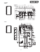
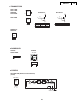
DN-C615
PCM 1716E (IC206)
BU2618FV (IC113)
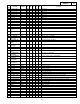
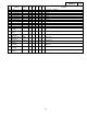
PIN NAME I/O DESCRIPTION
1 LRCIN IN Left and Right Clock Input. This clock is equal to
the sampling rate - f
S
.
(1)
2 DIN IN Serial Audio Data Input
(1)
3 BCKIN IN Bit Clock Input for Serial Audio Data.
(1)
4 CLKO OUT Buffered Output of Oscillator. Equivalent to
System Clock.
5 XTI IN Oscillator Input (External Clock Input)
6 XTO OUT Oscillator Output
7 DGND
-
Digital Ground
8V
DD
-
Digital Power +5V
9V
CC
2R
-
Analog Power +5V
10 AGND2R
-
Analog Ground
11 EXTR OUT Rch, Common Pin of Analog Output Amp
12 NC
-
No Connection
13 V
OUT
R OUT Rch, Analog Voltage Output of Audio Signal
14 AGND1
-
Analog Ground
15 V
CC
1
-
Analog Power +5V
16 V
OUT
L OUT Lch, Analog Voltage Output of Audio Signal
17 NC
-
No Connection
18 EXTL OUT Lch, Common Pin of Analog Output Amp
19 AGND2L
-
Analog Ground
20 V
CC
2L
-
Analog Power +5V
21 ZERO OUT Zero Data Flag
22 RST IN Reset. When this pin is low, the DF and
modulators are held in reset.
(2)
23 CS/IWO IN Chip Select/Input Format Selection. When this
pin is low, the Mode Control is effective.
(3)
24 MODE IN
Mode Control Select. (H: Software, L: Hardware)
(2)
25 MUTE IN Mute Control
26 MD/DM0 IN Mode Control, DATA/De-emphasis Selection 1
(2)
27 MC/DM1 IN Mode Control, BCK/De-emphasis Selection 2
(2)
28 ML/I
2
S IN Mode Control, WDCK/Input Format Selection
(2)
NOTES: (1) Pins 1, 2, 3; Schmitt Trigger input. (2) Pins 22, 24, 25, 26, 27,
28; Schmitt Trigger input with pull-up resister. (3) Pin 23; Schmitt Trigger
input with pull-down resister.
LRCIN
DIN
BCKIN
CLKO
XTI
XTO
DGND
V
DD
V
CC
2R
AGND2R
EXTR
NC
V
OUT
R
AGND1
ML/IIS
MC/DM1
MD/DM0
MUTE
MODE
CS/IWO
RST
ZERO
V
CC
2L
AGND2L
EXTL
NC
V
OUT
L
V
CC
1
1
2
3
4
5
6
7
8
9
10
11
12
13
14
28
27
26
25
24
23
22
21
20
19
18
17
16
15