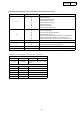
For U.S.A., Canada & Europe model SU PP SERVICE MANUAL MODEL DN-C680 LE ME NT Ver. 1 CD PLAYER We have two version of DN-C680. The new version of DN-C680 is replaced discontinued parts of the old version. (CD mechanism, microprocessor and D/A converter etc.) Serial number of new version are renumbered from *****50001. This service manual is supplement for new version of DN-C680 and only mentioned difference between old and new version.
DN-C680 SAFETY PRECAUTIONS The following check should be performed for the continued protection of the customer and service technician. LEAKAGE CURRENT CHECK Before returning the unit to the customer, make sure you make either (1) a leakage current check or (2) a line to chassis resistance check. If the leakage current exceeds 0.5 milliamps, or if the resistance from chassis to either side of the power cord is less than 460 kohms, the unit is defective.
DN-C680 BLOCK DIAGRAM ACD25 GU-3578-2 4M DRAM AN22002A ACD27 XCS05XL MN102H60KDA PCM1738 YM3437 RS-232C GU-3578-1 RS-422A RS-232C HD26C32A HD26LS31FP M66005AFP GU-3578-3 +7V_D1 +3.3V_D1 +6V +3.
DN-C680 4 CONFIRMING THE SERVO CAUTION: The Optical Pick-up used for CD player may invite defection by an external noise, such as electrostatic, etc., please pay the following attention. 1. Use a conductive mat on a working table to avoid electrostatic damage. 2. A working personnel should use a wrist strap to ground human body. 3. Tools, etc., specially for a soldering iron must use with its tip grounded and without leakage of electricity.
DN-C680 5 2. What is Service Program Service program is a special program intended for confirming servo. 3. Contents of Service Program While simultaneously pushing the STANDBY/CUE and PLAY/PAUSE buttons, turn the power on. (TRACK Indication “00”) After actuating the service program, select an aiming process number with the SELECT KNOB, PITCH button, and TIME button, and push the PLAY/PAUSE button to execute processing, The process number is then displayed on the TRACK indication portion. Work No.
DN-C680 Error Code Table (Appears only at Heat Run and Chucking Test function Error Code at TRACK portion Contents No.
DN-C680 7 CONFIRMING THE AUDIO 1. Necessary Equipment for Adjustment Distortion--Factor Meter VTVM Low-Pass Filter (20kHz) Reference Disc; DENON Audio Technical CD (38C39-7174) 2. Prior to Starting the Adjustment 1) Audio circuit shall be adjusted after adjustment of servo circuit. 3. Output Level Adjustment 1) Connect VTVM to the output connector of DN-C680.
DN-C680 SEMICONDUCTORS Only major semiconductors are shown, general semiconductors etc. are omitted to list. 主な半導体を記載しています。汎用の半導体は記載を省略しています。 1. IC’s Note : Abbreviation ahead of IC No. indicates the name of P.W.B., etc. 注 ) : IC No. の前の記号は、基板の名称を表します。 MA : Main P.W.B. DK : Display/Key P.W.B. MN102H60KDA (MA: IC137) 75 51 50 76 100 26 25 1 MN102H60KDA Terminal Function Pin No.
DN-C680 Pin No. Port Name Symbol I/O DET Ext Res Ini Note 29 A7 A7 O - - Unfix - Address bus 30 A8 A8 O - - Unfix - Address bus 31 A9 A9 O - - Unfix - Address bus 32 A10 A10 O - - Unfix - Address bus 33 A11 A11 O - - Unfix - Address bus 34 AVdd AVdd - - - - - Analog power supply(+3.
DN-C680 Pin No.
DN-C680 XCS05XL-5VQ100C (MA: IC112) 75 51 50 76 100 26 25 1 XCS05XL-5VQ100C Terminal Function Pin No. Port Name Symbol I/O Ext Note 1 GND GND - - 2 I/O,GCK1 I/O - - GND(0V) 3 I/O -PRST I Pd 4 I/O,TDI I/O - - Not used. Open 5 I/O,TCK I/O - - Not used. Open 6 I/O,TMS I/O - - Not used. Open 7 I/O -R I Pu Read signal 8 I/O -W I Pu Write signal Not used.
DN-C680 Pin No. Port Name Symbol I/O Ext 36 I/O(-INIT) -INIT O Pu 37 VCC VCC - - 38 GND GND - - 39 I/O PDI5 I Pu Note FPGA(XCS05XL) control signal:-INIT Power supply(+3.
DN-C680 Pin No. Port Name Symbol I/O Ext Note 91 I/O KI0 I Pu Key matrix data bus 92 I/O KI1 I Pu Key matrix data bus 93 I/O KI2 I Pu Key matrix data bus 94 I/O KI3 I Pu Key matrix data bus 95 I/O KI4 I Pu Key matrix data bus 96 I/O KI5 I Pu Key matrix data bus 97 I/O KI6 I Pu Key matrix data bus 98 I/O KI7 I Pu Key matrix data bus(Not used) 99 I/O,GCK8 I/O - - Not used. Open 100 VCC VCC - - Power supply(+3.
DN-C680 MN19412A (MA: IC126) MN19412A (Mecha Unit) (IC104) 43 63 64 42 84 22 1 21 MN19412A Terminal Function Pin No. 1 2 3 4 5 6 7 8 9 10 11 12 13 14 15 16 17 18 19 20 21 22 23 24 25 26 27 28 29 30 Symbol N.C. SOEN2 SCKO2 SDO3 WSO3 SCKO3 SOEN3 Vss Vss XCAS XOE A14 A13 A12 A11 A10 A9 A8 A7 A6 N.C. A5 A4 A3 A2 A1 A0 XCE2 XCE1 XRAS I/O/T — I I O/T I I I — — O O O O O O O O O O O — O O O O O O O O O Function Non connection. Output enable for serial output 2. Serial clock for serial output 2.
DN-C680 Pin No. 31 32 33 34 35 36 37 38 39 40 41 42 43 44 45 46 47 48 49 50 51 52 53 54 55 56 57 58 59 60 61 62 63 64 65 66 67 68 69 70 71 72 73 74 75 76 77 78 79 80 81 82 83 84 Symbol XWE VSS VSS D7 D6 D5 D4 D3 D2 D1 D0 P7 P6 P5 P4 P3 P2 P1/PT1 P0/PT0 N.C. SYNC VDD INT0 INT1 XRESET Vss CLKI CLKO VDD VDD ADDR0 ADDR1 XCE IICSEL XTRANS SDA SCL MATCH SDI1 WSI1 N.C. SCKI1 SDI2 WSI2 SCKI2 VDD VDD SDO1 WSO1 N.C.
DN-C680 MN662724 (MA: IC114) 41 60 61 40 80 21 1 MN662724 Pin No. 20 Terminal Function Symbol I/O O Function 1 BCLK Bit clock output for SRDATA. 2 LRCK O L,R discrimination signal output. 3 SRDATA O Serial data output. 4 DVDD1 Power supply for digital circuit. 5 DVSS1 GND for digital circuit. 6 TX O Digital audio interface output signal. 7 MCLK I Microcomputer command clock signal input (latches data at rising edge). 8 MDATA I Microcomputer command data input.
DN-C680 Pin No. Symbol I/O Function 36 OFT I Off track signal input ("H": off track). 37 TRCRS I Track cross signal input. 38 RFDET I RF detecting signal input ("L": detect). 39 BDO I Drop out signal input ("H": drop out). 40 LDON O Laser ON signal output ("H": ON). 41 PLLF2 I/O Loop filter terminal for PLL. 42 PLAY O Play signal output ("H": play). 43 WVEL O Double speed status signal output. 44 ARF I RF signal input. 45 IREF I Reference current input terminal.
DN-C680 M66005AFP (DK: IC502) AN22002A (MA: IC110) CAGC ARF 1 5 4 RFOUT 32 RF_EQ A + C 6 7 RFIN RFN CBD0 BD0 C0FTR 0FTR 12 11 8 AGC BD0 NRFDET 13 14 0FTR 9 3TENV - 15 + A C + - 22 31 E - 30 AMP GCA BCA AMP GCA BCA - 23 21 29 27 + F 28 AMP SUB - 20 + + 17 18 - + LD 25 FBAL 26 TBAL PD 24 16 3 GND VCC 18 NRFDET FEN FEOUT TEN TEOUT 19 VDET VREF 3TOUT TEBPF BCA GCA GCTL E BCA SUB B D F GCA + - AMP + 17 32 - 16 B + D CEA 1
DN-C680 W29C020C-90B (MA: IC106) W29C020C-90B Terminal Function SYMBOL NC 1 32 VDD A16 2 31 WE A15 3 30 A17 A12 4 29 A14 A7 5 28 A13 A6 6 27 A8 A5 7 26 A9 A4 8 25 A11 A3 9 24 OE A2 10 23 A10 A1 11 22 CE A0 12 21 DQ7 DQ0 13 20 DQ6 DQ1 14 19 DQ5 DQ2 15 18 DQ4 GND 16 17 DQ3 A0−A17 DQ0−DQ7 PIN NAME Address Inputs Data Inputs/Outputs CE Chip Enable OE Output Enable WE Write Enable VDD Power Supply GND Ground NC No Connection PCM1738-1
DN-C680 PVCC2 PGND2 D4+ D4- D 3+ D3- D 2+ D2- D 1+ D1- PGND1 PVCC1 AN8389 (MA: IC111) 24 23 22 21 20 19 18 17 16 15 14 13 thermal Protect Vcc Monitor BLT Linear Driver ch4 BLT Linear Driver ch3 BLT Linear Driver ch2 BLT Linear Driver ch1 ch4 Absolute V-I Direction Det ch3 Absolute V-I Direction Det ch2 Absolute V-I Direction Det ch1 Absolute V-I Direction Det VREF Monitor 5 6 7 8 VREF IN4 IN3 GND NC VRESET GND 9 10 11 12 PC1 4 IN1 3 PC2 2 IN2 1 VCC
DN-C680 21 SN74HCT244APW (MA: IC118,121,124,134-136,140,141) logic symbol Function Table INPUTS µ SN74LV245APW (MA: IC102,103,107,127) DiR 1 A Y H H L L L H X Z VDD 1 20 C4+ + C1 19 OE A1 3 G L µPD4721GS (MA: IC811) 20 VCC A0 2 OUTPUT 18 B0 2 19 GND VCC 3 18 C4- C1- 4 17 VSS C5+ 5 16 STBY 15 VCHA 14 DOUT1 13 DOUT2 A2 4 17 B1 A3 5 16 B2 A4 6 15 B3 DIN1 7 A5 7 14 B4 DIN2 8 A6 8 13 B5 ROUT1 9 5.5kohm A7 9 12 B6 ROUT2 10 5.
DN-C680 MM74HC4053SJ (MA: IC117) SN74HC157NS (MA: IC130) 16 VDD BY 1 IN/OUT BX 2 BX CY 3 CY OUT/IN C 4 IN/OUT CX 5 INH 6 VEE 7 BY B 15 B A 14 A AY 13 AY CX AX 12 AX 1A 1B 3 1B 4A 14 4A OUTPUT 1Y 4 1Y 4B 13 4B 2A 5 2A 4Y 12 4Y OUTPUT 2B 6 2B 3A 11 3A 2Y 3Y 3B 10 3B INPUTS IN/OUT INPUTS INH A 11 A VEE C B 10 B OUTPUT 2Y 7 9 C GND 8 INPUTS INPUTS 9 3Y OUTPUT 14 VCC 13 2CLR CK D PR CLR Q Q 12 2D 1PR 4 11 2CK 1Q 5 10 2PR 1Q 6 15 STROBE G BA6287F (MA
DN-C680 23 G R ID A S S IG N M E N T D A T E D p A N O D E C O N N E C T IO N 1 -1 2 -1 3 -1 4 -1 5 -1 1 -2 2 -2 3 -2 4 -2 5 -2 P 1 1 -1 T R A C K 1 -3 2 -3 3 -3 4 -3 5 -3 P 2 2 -1 4 d 4 d 5 -4 P 3 3 -1 3 d P 4 4 -1 P 5 1 -4 2 -4 3 -4 4 -4 1 -5 2 -5 3 -5 4 -5 5 -5 1 -6 2 -6 3 -6 4 -6 5 -6 1 -7 2 -7 3 -7 4 -7 5 -7 (1 G ~ 1 2 G , 1 9 G ) 1 G ~ 1 2 G 1 3 G 1 4 G 1 5 G 1 6 G 1 7 G 1 8 G 1 9 G B 1 1 B 1 1 1 -1 4 d B 1 0 B 1 0 2 -1 3 d 3
DN-C680 A N O D E C O N N E C T IO N 1 G ~ 1 2 G 1 3 G 1 6 G 1 5 G 1 4 G 1 7 G 24 1 8 G P 3 6 5 d P 3 7 4 d 4 d P 3 8 3 d 3 d P 3 9 2 d 2 d m s P 4 0 1 d 1 d 1 d P 4 1 5 e f P 4 2 4 e 4 e P 4 3 P 4 4 3 e 3 e 2 e 2 e P 4 5 1 e 1 e 1 e P 4 6 5 c T O C P 4 7 4 c 4 c P 4 8 3 c 3 c P 4 9 2 c 2 c P 5 0 1 c 1 c 1 c P 5 1 5 g E D IT P 5 2 4 g 4 g P 5 3 3 g 3 g P 5 4 2 g 2 g P 5 5 1 g 1 g 1 g P 5 6
DN-C680 PRINTED WIRING BOARDS GU-3001 DISPLAY/KEY P.W.B.
DN-C680 FOIL SIDE 26 26
DN-C680 GU-3578 MAIN P.W.B.
DN-C680 FOIL SIDE 28 28
DN-C680 29 NOTE FOR PARTS LIST l Part indicated with the mark " " are not always in stock and possibly to take a long period of time for supplying, or in some case supplying of part may be refused. l When ordering of part, clearly indicate "1" and "I" (i) to avoid missupplying. l Ordering part without stating its part number can not be supplied. l Part indicated with the mark " " is not illustrated in the exploded view. l Not including Carbon Film Resister ±5%, 1/4W Type in the P.W.Board parts list.
DN-C680 30 PARTS LIST OF P.W.B. UNIT *本表に記載されている部品は、補修用部品のため製品に使用している部品とは一部、形状、寸法などが異なる場合があります GU-3001B DISPLAY/KEY P.W.B. UNIT ASS'Y Ref.No. Part No.
DN-C680 Ref.No. Part No. Part Name Remarks OTHER PARTS GROUP ! CW051 203 8273 014 CW052 203 8224 018 5P KR-DS CON CORD 5P PH-SAN CON CORD CW071 204 2382 001 7P KR-DS CON.CORD CW091 204 2747 015 9P EH-SCN CONN CORD CW101 204 2412 036 10P KR-DS CONN CORD CX031 205 0581 001 2P VH CONNECTOR BASE CY241 205 0856 930 24P FFC CON.
DN-C680 32 GU-3578 MAIN P.W.B. UNIT ASS'Y Ref.No. Part No.
DN-C680 Ref.No. Part No.
DN-C680 Ref.No. C135 Part No.
DN-C680 Ref.No. Part No.
DN-C680 Ref.No. Part No.
DN-C680 Ref.No. Part No.
DN-C680 Ref.No. CY251 Part No.
DN-C680 39 EXPLODED VIEW Parts List 113 107 106 WARNING: Parts marked with this symbol have critical characteristics. Use ONLY replacement parts recommended by the manufacturer.
DN-C680 40 PARTS LIST OF EXPLODED VIEW *本表に記載されている部品は、補修用部品のため製品に使用している部品とは一部、形状、寸法などが異なる場合があります。 Note: The symbols in the column "Remarks" indicate the following destinations. E3: U.S.A. & Canada model E2: Europe model Ref.No. Part No.
DN-C680 Ref.No. Part No.
DN-C680 42 EXPLODED VIEW OF CD MECHANISM UNIT (CD11FTA3N) 4 3 20 17 3 16 8 16 7 11 2 6 12 1 10 5 15 9 18 13 14 19 PARTS LIST OF CD MECHANISM UNIT Ref. No. Part No. Part Name Remarks Q'ty Ref. No. Part No.
DN-C680 43 PACKING VIEW 203 ~ 206 202 207 201 202 208 210 211 210 PARTS LIST OF PACKING & ACCESSORIES *本表に記載されている部品は、補修用部品のため製品に使用している部品とは一部、形状、寸法などが異なる場合があります。 Note: The symbols in the column "Remarks" indicate the following destinations. E3: U.S.A. & Canada model E2: Europe model Ref.No. Part No. Part Name Remarks Q'ty 201 505 8092 007 LAMINATE ENVELOPE 1 202 503 1240 009 CUSHION 2 203 505 0038 030 POLY COVER 2 204 511 4101 007 INST.MANUAL 1 205 515 0945 007 WARRANTY (COM.
DN-C680 5P_KR WIRING DIAGRAM LDIN GND_A3 LDOUT LOAD+ LOAD- 6P_KR GU-3578-1 CX161 16P FFC GU-3578-2 7P EH 10P EH 7P EH CX104 CX072 GU-3578-3 44 +5V_A1 +12V_A1 -12V_A1 LOUT GND_A1 ROUT AMUTE CY072 10P EH -HB F1 F2 GND_A3 +7V_D1 GND_D1 +3.
DN-C680 NOTE FOR SCHEMATIC DIAGRAM 45 配線図について WARNING: Parts marked with this symbol ! have critical characteristics. Use ONLY replacement parts recommended by the manufacturer. ! 印の部品は安全を維持するために重要な部品です。 従って交換時は必ず指定の部品を使用してください。 注) CAUTION: (1) 指定なき抵抗値は Ω、k は kΩ、M は MΩ を示す。 Before returning the unit to the customer, make sure you make either (1) a leakage current check or (2) a line to chassis resistance check. If the leakage current exceeds 0.
DN-C680 SCHEMATIC DIAGRAMS (1/4) 1 2 3 4 5 6 7 8 9 10 46 11 A B C D E F G SIGNAL LINE SCHEMATIC DIAGRAMS (1/4) GU-3578-1 MAIN UNIT H 46
DN-C680 SCHEMATIC DIAGRAMS (2/4) 1 2 3 4 5 6 7 8 9 10 47 11 A B C D E F G SIGNAL LINE SCHEMATIC DIAGRAMS (2/4) GU-3578-2 DIGITAL I/F UNIT H 47
DN-C680 SCHEMATIC DIAGRAMS (3/4) 1 2 3 4 5 6 7 8 9 10 48 11 A B C D E F G SIGNAL LINE SCHEMATIC DIAGRAMS (3/4) GU-3578-3 AUDIO UNIT H 48
DN-C680 SCHEMATIC DIAGRAMS (4/4) 1 2 3 4 5 6 7 8 9 10 49 11 A B C D E F G SCHEMATIC DIAGRAMS (4/4) SIGNAL LINE GU-3001-1 KEY LED UNIT GU-3001-2 FLT UNIT GU-3001-3 H/P UNIT GU-3001-4 JOG SHUTTLE UNIT GU-3001-6 SELECT SW UNIT GU-3001-7 TRANS UNIT H 49