For U.S.A., Canada, Europe & Asia model Hi-Fi Component SERVICE MANUAL MODEL DN-D9000 DOUBLE CD PLAYER Some illustrations using in this service manual are slightly different from the actual set.
DN-D9000 SAFETY PRECAUTIONS The following check should be performed for the continued protection of the customer and service technician. LEAKAGE CURRENT CHECK Before returning the unit to the customer, make sure you make either (1) a leakage current check or (2) a line to chassis resistance check. If the leakage current exceeds 0.5 milliamps, or if the resistance from chassis to either side of the power cord is less than 460 kohms, the unit is defective.
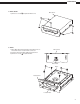
DN-D9000 DISASSEMBLY (Follow the procedure below in reverse order when reassembling) Main Unit 1. Drive Unit 1) Remove 4 screws 1 and pull out Drive Unit. 2) Disconnect Flat cable and Connector. 3) Detach Drive Unit. 1 1 Drive Unit Note: • Pull at a straight angle to avoid Flat Cable damage. • Do not fail to pull AC cord from wall outlet before disconnect the Flat Cable and Connector. If AC cord is remained plugged into wall outlet, power is kept supplied in the unit, which may cause danger.
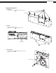
DN-D9000 4. Drive Cover 1) Remove 5 screws 5 Drive Cover and pull out Drive Cover. 5 5 5. Drive 1) Move Drive Rack in arrow direction through the hole on the bottom chassis. Loader Frame comes out. 2) Pull up Loader Panel while pulling it towards front. 3) Remove 4 screws 6 and pull out Drive.
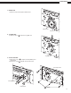
DN-D9000 Remote Control Unit 1. Top Cover 7 1) Remove 7 screws 7 and pull out Top Cover. Top Cover 2. Cover 1) Disconnect Connector. 2) Remove 2 screws 8 and pull out Cover. Connector Cover 8 3. Sensor Unit 1) Remove 2 screws 9 and pull out Sensor Cover. 2) Detach Sensor Unit.
DN-D9000 4. Wheel Unit 1) Remove Set Screw and pull out Wheel Unit. Wheel Unit Set Screw 5. Jog Dial Unit 1) Remove a E ring and pull out Jog Dial Unit. Jog Dial Unit 6. Inner Panel Unit 1) Remove 4 screws Fader Knob. 2) Remove 4 screws and pull out Knob (MARU) and and pull out Inner Panel Unit.
DN-D9000 BLOCK DIAGRAM 1 2 3 4 5 6 DN-D9000 7 8 RC-D90 CD1 A FLT Driver 128MB SDRAM FG-9000 DRIVE1 FL tube out D6~D31 ADDRESS ADSP21065L 128MB SDRAM ATAPI INTERFACE main1 out LRCK BCLK MAIN1 MON1 TFS0 TCK0 TXD0A TXD0B ML9207 AMP10 8CH D/A PCM1608 DSP1 CD1 µcom mon1 out AMP11 main2 out SHOCK PROOF LEDdrive AMP20 BU2090 TMP86CM47U ROM32k RAM1k mon2 out BUS select ATAPI interface 16Bit Bus D0~D15 EFFECTOR TFS1 TCK1 DIT SM5902 DOUT1 TXD1A 384fs AMP21 RAM Control FLT1
DN-D9000 CONFIRMING THE SERVO Required Measuring Implement 1. Reference disc (TCD784 or CO-74176) 1. What is Service Program Service program is a special program intended for confirming servo functions etc. 2. Contents of Service Program Switch on the power while pushing the CD1’s PITCH BEND + button and CD2’s α CUE button at the same time. After actuating the servo program, select an aiming process number with the SELECT knob, A1 button, A2 button, or A3 button.
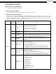
DN-D9000 Adjustment Item 1 2 3 4 5 6 Focus Gain Focus Balance Focus Offset Tracking Gain Tracking Balance Tracking Offset Adjustment Value indication at character portions. 35 ~ 120 20 ~ 20 20 ~ 20 35 ~ 120 20 ~ 20 20 ~ 20 * Reference data. 3. TEST MODE Process No. (TRACK Indication) A1 button A2 button Function Contents (Character-display) Heat Run Chucking Test (H/R1_Normal) (H/R2_Tray) Starting with the PLAY/PAUSE button, it repeats open/close of the tray and playback.
DN-D9000 Detailed error can be displayed by JOG dial when error occurs. Error Indication TR MIN Displays the track No. in which error occurred. SEC FRAM Displays the time at which error occurred. CHARACTER “H uuuu E uuu” Operation count Error code 5. System µcom and DSP Version Upgrade System µcom and DSP can be upgraded in the following manner. Version Upgrade Method 1. Record the version upgrade software on a CD-R or CD-RW disc, only as one file with the format ISO9660 Mode-1.
DN-D9000 SEMICONDUCTORS IC’s Note: Indication before IC Numbers denotes P.W.B. name. FG : CD-ROM P.W.B. Unit DS : DSP P.W.B. Unit PO : Power P.W.B. Unit RC : Remote P.W.B. Unit MN102H730F (DS: IC501) 96 65 97 64 TOP VIEW 128 33 1 32 MN102H730F Terminal Function Pin No.
DN-D9000 Pin No.
DN-D9000 Pin No.
DN-D9000 ADSP-21065L (DS: IC301, 401) 208 157 156 1 TOP VIEW 52 105 104 53 ADSP-21065L Terminal Function Pin No.
DN-D9000 Pin No.
DN-D9000 Pin No.
DN-D9000 Pin No.
DN-D9000 TMP86CM47U (DS: IC101, 151) 23 33 34 22 TOP VIEW 44 12 1 11 TMP86CM47U Terminal Function Pin No.
DN-D9000 SM5902AF (DS: IC651, 652) 23 33 34 22 TOP VIEW 44 SM5902AF Terminal Function Pin No.
DN-D9000 ML MC MDI MDO ZERO8 DATA4 ZERO7 NC VCC1 AGND1 VCC2 AGND2 PCM1608Y (DS: IC705) 36 35 34 33 32 31 30 29 28 27 26 25 RST SCKI SCKO BCK LRCK TEST VDD DGND DATA1 DATA2 DATA3 ZEROA 37 38 39 40 41 42 43 44 45 46 47 48 24 23 22 21 20 19 18 17 16 15 14 13 TOP VIEW VCC3 AGND3 VCC4 AGND4 VOUT8 AGND6 VCC5 AGND5 VOUT7 VCOM VOUT1 VOUT2 ZERO1/GPO1 ZERO2/GPO2 ZERO3/GPO3 ZERO4/GPO4 ZERO5/GPO5 ZERO6/GPO6 NC NC VOUT6 VOUT5 VOUT4 VOUT3 1 2 3 4 5 6 7 8 9 10 11 12 BCK DAC Output Amp and Low-Pass Filter VOU
DN-D9000 Pin No. 11 12 13 14 15 16 17 18 19 20 21 22 23 24 25 26 27 28 29 30 31 32 33 34 35 36 37 38 39 40 41 42 43 44 45 46 47 48 Pin Name VOUT4 VOUT3 VOUT2 VOUT1 VCOM VOUT7 AGND5 VCC5 AGND6 VOUT8 AGND4 VCC4 AGND3 VCC3 AGND2 VCC2 AGND1 VCC1 NC ZERO7 DATA4 ZERO8 MDO MDI MC ML RST SCKI SCKO BCK LRCK TEST VDD DGND DATA1 DATA2 DATA3 ZEROA I/O O O O O O O — — — — — — — — — — — — — — — — O l l l l l O l l — — — l l l O Function Voltage Output of Audio Signal Corresponding to Rch on DATA2.
DN-D9000 AD2 AD1 VDISP2 NC VFL2 P4 P3 P2 P1 VDD DA CP CS RESET OSC1 OSC0 GND VFL1 COM24 COM23 ML9207-01GP (RC: IC101, 201) 80 79 78 77 76 75 74 73 72 71 70 69 68 67 66 65 64 63 62 61 AD3 AD4 SEG1 SEG2 SEG3 SEG4 SEG5 SEG6 SEG7 SEG8 SEG9 SEG10 SEG11 SEG12 SEG13 SEG14 SEG15 SEG16 SEG17 SEG18 1 2 3 4 5 6 7 8 9 10 11 12 13 14 15 16 17 18 19 20 60 59 58 57 56 55 54 53 52 51 50 49 48 47 46 45 44 43 42 41 TOP VIEW COM22 COM21 COM20 COM19 COM18 COM17 COM16 COM15 COM14 COM13 COM12 COM11 COM10 COM9 COM8 COM7 CO
DN-D9000 TMP86CM47U (RC: IC102, 202) 23 33 34 22 TOP VIEW 44 12 1 11 TMP86CM47U Terminal Function Pin No.
XSAWRCVCO XSVREFO XSPDOFTR2 XSVR_PLL XSFTROPI XSFDO AVSS_PL XSPLLFTR2 AVDD5_PL XSFDIREF XSPDIREF GND XTSLRF XTPLCK VDD XRA(3) XRA(2) XRA(1) XRA(0) XRA(4) XRA(5) XRA(6) GND XRA(7) XRA(10) XRA(11) VDD XRA(8) XRA(9) XROEJ VDD XRCASJ XRRASJ XRSDCLK XRWEJ XRD(7) XRD(8) XRD(6) GND XRD(9) XRD(5) XRD(10) XRD(4) XRD(11) DN-D9000 176 175 174 173 172 171 170 169 168 167 166 165 164 163 162 161 160 159 158 157 156 155 154 153 152 151 150 149 148 147 146 145 144 143 142 141 140 139 138 137 136 135 134 133 M5705 (FG:
DN-D9000 Pin No.
DN-D9000 Pin No. Pin Name Type Description This pin is used as the Passed Diagnostics signal, and may be an input or an open-drain output This pin is used as the Drive Active/Slave Present signal, and is an input or an open-drain output. This pin is used for Master/Slave drive communication and/or for driving an LED 1. I/O channel ready. This signal is driven low to extend host transfer cycles when the controller is not ready to respond.
DN-D9000 HOLD1 VNA FNN FNP DIP DIN RX BYP SIGO VPA AIP AIN ATON ATOP CDRF CDRDDC SP3721A (FG: IC502) 64 63 62 61 60 59 58 57 56 55 54 53 52 51 50 49 DVDRFP 1 48 SDEN DVDRFN 2 47 SDATA PD1 3 46 SCLK PD2 4 45 LCP A2 5 44 LCN B2 6 43 CE C2 7 42 FE D2 8 CP 9 41 TE TOP VIEW 40 MEI CN 10 39 MEV D 11 38 TPH C 12 37 DFT B 13 36 PI A 14 35 MIN F 15 34 MEVO E 16 33 MLPF FDCHG# VIB VIP VIIRR VPB VCI VC LDON# CDLD CDPD DVDLD DVDPD VNB NC VCI2 CD
DN-D9000 Type Description 43 34 Pin No. CE NEVO O O 37 DFT O 29 MIRR O 36 PI O 22 24 56 DVDLD CDLD BYP O O I/O 9 CP I/O 10 CN I/O 45 44 30 31 39 17 38 LCP LCN MP MB MEV CDTE TPH — — — — — — — 26 VC — 27 18 VCI VCI2 — — 55 RX — 33 19 MLPF NC — — 48 SDEN I 47 SDATA I/O 46 SCLK I 58 28 50 20 VPA VPB VNA VNB Center Error Signal Output. Center error output reference to VCI SIGO Bottom Envelope Output. Bottom envelope for mirror detection Defect Output.
DN-D9000 128M SDRAM (DS: IC302, 303, 402, 403) 1 Pin Assignment 54 Pin No. 22, 23~26, 29~35 20, 21 Pin Name Function A0~A11 Address BS0, BS1 2, 4, 5, 7, 8, DQ0~ 10,11, 13, 42, DQ15 44,45, 47, 48, 50, 51, 53 19 CS# TOP VIEW 27 18 RAS# 17 16 15, 39 CAS# WE# UDQM/ LDQM 38 37 CLK CKE 1, 14, 27 28, 41, 54 3, 9, 43, 49 6, 12, 46, 52 36, 40 Vcc Vss VccQ VssQ NC 28 Description Multiplexed pins for row and column address. Row address: A0~A11. Column address: A0~A8.
DN-D9000 BD6670FM Terminal Function BD6670FM (FG: IC510) Pin Pin No.
DN-D9000 M11B416256A-35J (FG: IC508) VCC I/O0 I/O1 I/O2 I/O3 VCC I/O4 I/O5 I/O6 I/O7 NC NC WE RAS NC A0 A1 A2 A3 VCC 1 2 3 4 5 6 7 8 9 10 11 12 13 14 15 16 17 18 19 20 TOP VIEW SN74AHC245APW (RC: IC301) SN74LV245APW (DS: IC103, 104, 153, 154, 504-507, 601, 707) 40 39 38 37 36 35 34 33 32 31 30 29 28 27 26 25 24 23 22 21 VSS I/O15 I/O14 I/O13 I/O12 VSS I/O11 I/O10 I/O9 I/O8 NC CASL CASH OE A8 A7 A6 A5 A4 VSS DiR 1 18 B0 A2 4 17 B1 A3 5 16 B2 A4 6 15 B3 A5 7 14 B4 A6 8 13 B5 A7 9 12 B6 GND
DN-D9000 STR-F6676 (PO: IC901) BA033T (PO: IC905) NJM7805FA (DS: IC605) (RC: IC312) VIN 4 FRONT VIEW FRONT VIEW R3 100Ω 3 D R4 O.V.P LATCH DRIVE 2 S REG. O.C.P./F.B. S D VIN GND 20Ω Input GND Output START Vth(1) 1 O.C.P/F.B Comp.1 O.S.C T.S.D Iconst Vth(2) Comp.
DN-D9000 ' TRANSISTORS 2SB1328 (P) 2SD2004 (P) 2SA1036K 2SC2411K KTC2875B FRONT VIEW 2SK2414 2SB766S 2SB1132 D C FRONT VIEW B TOP VIEW TOP VIEW C E E C B B C E G D S DTA114EK DTC114EK DTC143EK DTA114EK DTC114EK DTC143EK PNP Type B NPN Type C R1 R1 TOP VIEW C C B B R1 R2 R1 E R2 DTC114EK 10kohm 10kohm DTA114EK 10kohm 10kohm R2 R2 DTC143EK 4.7kohm 4.7kohm E E ' DIODES (included LED) 1SR35-400A 1SS133 1SS270A AG01ZT (V1) AL01ZT (V1) SARS01T (V1) RK14 RK44 RK46 MTZJ3.
DN-D9000 ' FL DISPLAY 24-ST-09GN (RC: FL102, 202) 82 51 44 1 Pin Connection 8 8 8 8 8 8 8 8 7 6 5 4 3 2 P Connection N N N N N N 2 PPPPPP 0 8 1 P 1 9 8 0 P 1 8 7 9 P 1 7 7 8 P 1 6 7 7 P 1 5 7 6 P 1 4 7 5 P 1 3 7 4 P 1 2 7 3 P 1 1 7 2 P 1 0 7 7 6 6 6 6 6 6 6 6 6 6 5 5 5 5 5 5 5 5 5 5 1 0 9 8 7 6 5 4 3 2 1 0 9 8 7 6 5 4 3 2 1 0 1 2 2 PPPPPPPPP 0 9 8 7 6 5 4 3 2 1 3 4N 9 8 7 6 5 4 3 2 1 GGGGGGGGGGGGP 1 2 3 4 5 6 7 8 P Connection F F F F N N I 2 − − − − PPC1 9 P 2 2 1 0 P 2 3 1 1 P 2 4 1 2
DN-D9000 PRINTED WIRING BOARDS 1 4 3 2 5 6 7 8 GU-3412 DSP P.W.B.
DN-D9000 1 2 4 3 5 6 7 8 GU-3412 DSP P.W.B.
DN-D9000 1 4 3 2 5 6 7 8 GU-3413 POWER P.W.B.
DN-D9000 1 4 3 2 5 6 7 8 GU-3414 CD-ROM P.W.B.
DN-D9000 1 4 3 2 5 6 7 8 GU-3415 REMOTE P.W.B.
DN-D9000 NOTE FOR PARTS LIST l Part indicated with the mark " " are not always in stock and possibly to take a long period of time for supplying, or in some case supplying of part may be refused. l When ordering of part, clearly indicate "1" and "I" (i) to avoid mis-supplying. l Ordering part without stating its part number can not be supplied. l Part indicated with the mark " " is not illustrated in the exploded view. l Not including Carbon Film ±5%, 1/4W Type in the P.W.Board parts list.
DN-D9000 PARTS LIST OF P.W.B. UNIT ASS'Y GU-3412 DSP P.W.B. UNIT ASS'Y Ref. No. Part No. Part Name Remarks Ref. No. Part No.
DN-D9000 Ref. No. Part No. Part Name Remarks Ref. No. Part No.
DN-D9000 Ref. No. Part No. Part Name Remarks R762 247 2006 960 Carbon chip 470 ohm 1/16W RM73B--471JT R763-770 247 2003 947 Carbon chip 22 ohm 1/16W R771 247 2006 986 Carbon chip 470 ohm 1/16W RM73B--561JT R772 247 2014 965 Carbon chip 1 Mohm 1/16W R773-780 247 2005 987 Carbon chip 100 ohm 1/16W RM73B--221JT R782,783 247 2003 947 Carbon chip 22 ohm 1/16W RM73B--220JT RM73B--105JT Ref. No. C429-431 Part No. Part Name Remarks 257 0512 903 Ceramic chip 0.
DN-D9000 Ref. No. C669 Part No. Part Name Remarks Ref. No. Part No. Part Name Remarks Q'ty 257 0509 929 Ceramic chip 1000pF/50V CK73B1H102KT OTHER PARTS GROUP C670,671 257 0501 901 Ceramic chip 0.01µF/50V CK73B1H103KT (1608) CX061 205 0355 062 6P KR connector base (L) 1 C672 257 0512 903 Ceramic chip 0.1µF/25V CK73F1E104ZT CX131 205 0480 034 13P KR connector base (L) 1 C674 257 0512 903 Ceramic chip 0.
DN-D9000 GU-3413 POWER P.W.B. UNIT ASS'Y Ref. No. Part No. Part Name Remarks Note : The symbols in the column “Remarks” indicate the following destinations. E3 : U.S.A. & Canada model E2 : Europe model Ref. No. Part No.
DN-D9000 GU-3414 CD-ROM P.W.B. UNIT ASS'Y Ref. No. Part No. Part Name Remarks Ref. No. Part No.
DN-D9000 Ref. No. Part No. Part Name Remarks Ref. No. Part No. Part Name Remarks C507,508 257 0516 941 Ceramic chip 0.047µF/25V CK73B1E473KT 1608 C596 257 0512 903 Ceramic chip 0.1µF/25V CK73F1E104ZT 1608 C598-608 257 0512 903 Ceramic chip 0.1µF/25V CK73F1E104ZT 1608 C509,510 257 0516 954 Ceramic chip 0.1µF/25V CK73B1E104KT 1608 C511,512 257 0509 929 Ceramic chip 1000pF/50V CK73B1H102KT 1608 C513 257 0516 954 Ceramic chip 0.
DN-D9000 GU-3415 REMOTE P.W.B. UNIT ASS'Y Ref. No. Part No. Part Name Remarks Ref. No. Part No.
DN-D9000 Ref. No. Part No. Part Name Remarks Ref. No. Part No.
DN-D9000 Ref. No. Part No. Part Name C123-126 257 0511 920 Ceramic chip 0.047µF/50V Remarks Ref. No. Part No. Part Name CK73F1H473ZT C327 253 9039 906 Ceramic 0.1µF/25V Remarks CK45=1E104ZT(DD-3) C127 257 0512 903 Ceramic chip 0.1µF/25V CK73F1E104ZT C328 253 9037 908 Ceramic 0.1µF/50V CK45=1H104ZT(BC) C128 257 0501 901 Ceramic chip 0.01µF/50V CK73B1H103KT (1608) C329 254 4592 904 Electrolytic 120µF/16V CE04W1C121MTF11(LXV) CE04W1H560MCF15(LXV) C129 257 0512 903 Ceramic chip 0.
DN-D9000 EXPLODED VIEW OF REMOTE CONTROL UNIT (RC-D90) 1 4 3 2 5 6 7 8 54 54 A 54 20 54 25 55 22 22 23 18 B 24 16 17 32 21 1-3 1-1 58 52 31 54 71 63 7 58 60 19 52 31 56 72 63 9 C 6 60 3 8 2 5 15 1-2 56 7 1-4 1-5 10 3 59 4 51 9 6 52 8 10 5 D 26 53 27 14 13 12 26 58 61 53 60 27 11 E 59 51 51 5
DN-D9000 PARTS LIST OF REMOTE CONTROL UNIT (RC-D90) Ref. No. Part No. Part Name 1 1-1 1-2 1-3 1-6 1-7 GU-3415 − − − − − Remote P.W.B. unit Ass'y Panel P.W.B. unit Panel P.W.B. unit Connect P.W.B. unit Sensor P.W.B. unit Sensor P.W.B.
DN-D9000 EXPLODED VIEW OF MAIN UNIT 1 4 3 2 5 6 7 WARNING: Parts marked with this symbol have critical characteristics. Use ONLY replacement parts recommended by the manufacturer.
DN-D9000 Note : The symbols in the column “Remarks” indicate the following destinations. E3: U.S.A. & Canada model E2: Europe model PARTS LIST OF MAIN UNIT Ref. No. Part No. Part Name 1 2 2-1 2-2 2-3 GU-3412 GU-3413 − − − DSP P.W.B. unit Ass'y Power P.W.B. unit Ass'y Power P.W.B. unit OP/CL switch P.W.B. unit LED P.W.B.
DN-D9000 EXPLODED VIEW OF CD DRIVE UNIT (FG-9000) 1 4 3 2 12 11 A 12 6 6 B 1 12 C 13 3 2 16 4 Puts Item 7 according to this line.
DN-D9000 PARTS LIST OF CD DRIVE UNIT Ref. No. 1 2 4 7 8 10 11 13 16 21 22 Part No. Part Name 9KC 2A06 5A GU-3414 412 4924 000 415 0876 009 144 2799 004 475 1178 009 102 0657 005 146 2277 001 417 0630 005 513 2065 002 513 3797 007 CD mecha. Unit TD-5HP-D2 CD-ROM P.W.B.
DN-D9000 EXPLODED VIEW OF CD MECHANISM 1 4 3 2 5 6 7 8 14 69 26 3 A 27B 46 47 26 32 47 31 30 63 8 32 44 38 2 33 43 34 12 37 15 39 B 28 50 42 43 36 35 21 51 29 1 23 27 51 6 21 53 50 40 70 51 5 C 23 51 71 7 49 24 49 11 49 48 23 24 59 41 24 27A 49 24 D 9 10 17 24 16 4 25 18 64 22 20 E 19 57
DN-D9000 PARTS LIST OF CD MECHANISM UNIT Ref. No. Part No.
DN-D9000 POINTS OF GREASING 1 4 3 2 5 6 7 8 14 Greasing positions(groove) Froil KG-423 Tray bottom face , in 2 grooves , from 1st to 3rd tooth of gear (0.1mg each 3) TRAY bottom view 26 3-Bond 1401B More than half of the screw. 69 3 (2 position) 46 Sancoal LEN-315Y S-GUIDE BAR-84H Top and bottom all area. (0.2mg each 1) 26 A 47 47 31 32 3-Bond 1401B More than half of the screw. 8 30 63 32 44 2 Froil KG-423 Chassis L , 9 positions of rail hook. Chassis R , 9 positions of rail hook.
DN-D9000 PACKING VIEW 102 101 Remote controller 102 105 ~ 109 104 103 Main unit 104 111 Note : The symbols in the column “Remarks” indicate the following destinations. E3 : U.S.A. & Canada model E2 : Europe model PARTS LIST OF PACKING & ACCESSORIES Ref. No. Part No. Part Name Remarks Q'ty Ref. No. Part No.
DN-D9000 2 3 4 DN-D9000 DOUBLE CD PLAYER 1 2 3 4 5 6 7 8 9 10 11 12 13 14 15 FM+ FMSW SW H+ HH3H3+ H2H2+ H1H1+ A1 A2 A3 CY401 RES_ GND D7 D8 D6 D9 D5 D10 D4 D11 D3 D12 D2 D13 D1 D14 D0 D15 GND NC DMAREQ GND DIOW_ GND DIOR_ GND IORDY NC DMAACK GND INTRQ IOCS16 DA1 NC DA0 DA2 CS0 CS1 NC GND 1 2 3 4 5 6 7 8 9 10 11 12 13 14 15 16 17 18 19 20 21 22 23 24 25 26 27 28 29 30 31 32 33 34 35 36 37 38 39 40 CX401 1 RES_ 2 GND 3 D7 4 D8 5 D6 6 D9 7 D5 8 D10 9 D4 10 D11 11 D3 12 D12 13 D2 14 D13 15 D1 16 D14 1
DN-D9000 SCHEMATIC DIAGRAMS (1/6) 1 2 3 4 5 6 7 8 9 10 11 A B C D E F G WARNING: Parts marked with this symbol have critical characteristics. Use ONLY replacement parts recommended by the manufacture. CAUTION: NOTICE ALL RESISTANCE VALUES IN OHM. k=1,000 OHM M=1,000,000 OHM ALL CAPACITANCE VALUES IN MICRO FARAD. P=MICRO-MICRO FARAD EACH VOLTAGE AND CURRENT ARE MEASUERD AT MO SIGNAL INPUT CONDITION. CIRCUIT AND PARTS ARE SUBJECT TO CHANGE WITHOUT PRIOR NOTICE.
DN-D9000 SCHEMATIC DIAGRAMS (2/6) 1 2 3 4 5 6 7 8 9 10 11 A B C D E F NOTICE ALL RESISTANCE VALUES IN OHM. k=1,000 OHM M=1,000,000 OHM ALL CAPACITANCE VALUES IN MICRO FARAD. P=MICRO-MICRO FARAD EACH VOLTAGE AND CURRENT ARE MEASUERD AT MO SIGNAL INPUT CONDITION. CIRCUIT AND PARTS ARE SUBJECT TO CHANGE WITHOUT PRIOR NOTICE. G WARNING: Parts marked with this symbol have critical characteristics. Use ONLY replacement parts recommended by the manufacture.
DN-D9000 SCHEMATIC DIAGRAMS (3/6) 1 2 3 4 5 6 7 8 9 10 11 A B C D E F G WARNING: Parts marked with this symbol have critical characteristics. Use ONLY replacement parts recommended by the manufacture. + B LINE CAUTION: Before returning the unit to the customer, make sure you make either (1) a leakage current check or (2) a line to chassis resistance check. If the leakage current exceeds 0.
DN-D9000 SCHEMATIC DIAGRAMS (4/6) 1 2 3 4 5 6 7 8 9 10 11 A B C D E F WARNING: NOTICE Parts marked with this symbol have critical characteristics. Use ONLY replacement parts recommended by the manufacture. ALL RESISTANCE VALUES IN OHM. k=1,000 OHM M=1,000,000 OHM ALL CAPACITANCE VALUES IN MICRO FARAD. P=MICRO-MICRO FARAD EACH VOLTAGE AND CURRENT ARE MEASUERD AT MO SIGNAL INPUT CONDITION. CIRCUIT AND PARTS ARE SUBJECT TO CHANGE WITHOUT PRIOR NOTICE.
DN-D9000 SCHEMATIC DIAGRAMS (5/6) 1 2 3 4 5 6 7 8 9 10 11 A B C D E F G WARNING: _ B LINE + Parts marked with this symbol have critical characteristics. Use ONLY replacement parts recommended by the manufacture. CAUTION: NOTICE ALL RESISTANCE VALUES IN OHM. k=1,000 OHM M=1,000,000 OHM ALL CAPACITANCE VALUES IN MICRO FARAD. P=MICRO-MICRO FARAD EACH VOLTAGE AND CURRENT ARE MEASUERD AT MO SIGNAL INPUT CONDITION. CIRCUIT AND PARTS ARE SUBJECT TO CHANGE WITHOUT PRIOR NOTICE.
DN-D9000 SCHEMATIC DIAGRAMS (6/6) 1 2 3 4 5 6 7 8 9 10 11 A B C D E F NOTICE ALL RESISTANCE VALUES IN OHM. k=1,000 OHM M=1,000,000 OHM ALL CAPACITANCE VALUES IN MICRO FARAD. P=MICRO-MICRO FARAD EACH VOLTAGE AND CURRENT ARE MEASUERD AT MO SIGNAL INPUT CONDITION. CIRCUIT AND PARTS ARE SUBJECT TO CHANGE WITHOUT PRIOR NOTICE. WARNING: Parts marked with this symbol have critical characteristics. Use ONLY replacement parts recommended by the manufacture.