
User Guide


17
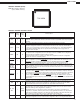
DN-V1700
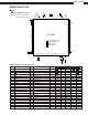
XCS30XL-4PQ208C (IC102)
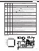
XCS30XL-4PQ208C Terminal Function
Pin DescriptionPin Name
I/O
During
Config.
I/O
After
Config.
TOP VIEW
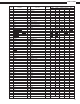
Permanently Dedicated Pins
Eight or more (depending on package) connections to the nominal +5V supply voltage (+3.3V for
VCC X X Spartan-XL devices). All must be connected, and each must be decoupled with a 0.01-0.1µF capacitor
to Ground.
GND X X Eight or more (depending on package) connections to Ground. All must be connected.
During configuration, Configuration Clock (CCLK) is an output in Master mode and is an input in Slave
mode. After configuration, CCLK has a weak pull-up resistor and can be selected as the Readback
CCLK I or O I Clock. There is no CCLK High or Low time restriction on Spartan/XL devices, except during Readback.
See Violating the Maximum High and Low Specification for the Readback Clock, page 39 for an
explanation of this exception.
DONE is a bidirectional with an optional internal pull-up resistor. As an open-drain output, it indicates
the completion of the configuration process. As an input, a Low level on DONE can be configured to
DONE I/O O delay the global logic initialization and the enabling of outputs.
The optional pull-up resistor is selected as an option in the program that creates the configuration
bitstream. The resistor is included by default.
PROGRAM is an active Low input that forces the FPGA to clear its configuration memory. It is used to
PROGRAM I I
initiate a configuration cycle. When PROGRAM goes High, the FPGA finishes the current clear cycle
and executes another complete clear cycle, before it goes into WAIT state and releases INIT. The
PROGRAM pin has a permanent weak pull-up, so it need not be externally pulled up to VCC.
MODE The Mode input(s) are sampled after INIT goes High to determine the configuration mode to be used.
(Spartan)
IX
During configuration, these pins have a weak pull-up resistor. For the most popular configuration mode,
M0, M1 Slave Serial, the mode pins can be left unconnected. For Master Serial mode, connect the Mode/M0 pin
(Spartan-XL)
directly to system ground.
PWRDWN is an active Low input that forces the FPGA into the Power Down state and reduces power
consumption. When PWRDWN is LOW, the FPGA disables all I/O and inititalizes all flip-flops. All inputs
are interpreted as Low independent of their actual level. VCC must be maintained, and the configuration
PWRDWN I I data is maintained. PWRDWN halts configuration if asserted before or during configuration, and
re-starts configuration when removed. When PWRDWN returns High, the FPGA becomes operational
by first enabling the inputs and flip-flops and then enabling the outputs. PWRDWN has a default internal
pull-up resistor.
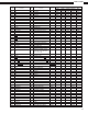
User I/O Pins That Can Have Special Functions
If boundary scan is used, this pin is the Test Data Output. If boundary scan is not used, this pin is a
TDO O O 3-state output without a register, after configuration is completed. To use this pin, place the library
component TDO instead of the usual pad symbol. An output buffer must still be used.
If boundary scan is used, these pins are Test Data In, Test Clock, and Test Mode Select inputs
respectively. They come directly form the pads, bypassing the IOBs. These pins can also be used as
TDI, TCK, I/O or I
inputs to the CLB logic after configuration is completed.
TMS
I
(JTAG)
If the BSCAN symbol is not placed in the design, all boundary scan functions are inhibited once
configuration is completed, and these pins become user-programmable I/O. In this case, they must be
called out by special library elements. To use these pins, place the library components TDI, TCK, and
TMS instead of the usual pad symbols. Input or output buffers must still be used.
HDC O I/O
High During Configuration (HDC) is driven High until the I/O go active. It is available as a control output
indicating that configuration is not yet completed. After configuration, HDC is a user-programmable I/O pin.
Note: When this IC is defective,
replace P.W.B. Unit Ass'y.