
User Guide


23
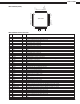
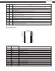
DN-V1700
Video
Inputs
LTC
Input
Processor
Bus
VITC
Receiver
Video
Timing &
Character
Generator
VITC
Generator
LTC
Generator
LTC
Receiver
Processor
Interface
Interrupt
Timer
UART
Video
Output
Video
Output
LTC Output
TxD, RxD
CTS, RTS
12
13
14 15 16 17 18 19 20 21 22
23
24
25
26
27
28
30
32
29
31
33
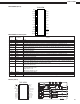
44 43 42 41 40 39 3435363738
D2
D1
D0
IOW*
VDD
VSS
IOR*
UARTCS*
SMPTEC*
A1
A0
Y
1
S
T
H
R
E
S
H
C
T
H
R
E
S
H
D
T
H
R
E
S
H
R
X
D
C
T
S*
T
X
D
R
T
S*
L
R
C
L
K
V
I
T
C
G
A
T
E
V
I
T
C
O
U
T
LTCOUT
LFC
XTAL2
XTAL1
AVD D
AVSS
COUT
YOUT
C2
Y2
C1
D
4
L
T
C
I
N
+
D
3
L
T
C
I
N
-
C
L
I
C
K
F
R
A
M
E
R
E
S
E
T
I
N
T
R
D
7
D
6
D
5
1
2
3
4
5
6
7
8
9
10
11
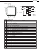
ICS2008BY-10 (IC501)
ICS2008BY Terminal Function
Pin
No.
Pin Name DescriptionType
12, 10 Y1, Y2 AI
Video inputs from camera or other source. NOTE: This is also the Y (Luma) input for S-VHS
and HI-8 systems.
11, 9 C1, C2 AI
C (Chroma) inputs for S-VHS and HI-8 systems. In NTSC systems, this pin should be tied to
its respective Y input.
15 DTHRESH AI Data Threshold bypass input.
13 STHRESH AI SYNC Threshold bypass input.
14 CTHRESH AI Clamp Threshold bypass input.
8 Y OUT AO Video output. This is also the Y (Luma) output in S-Video mode.
7 C OUT AO C (Chroma) output for S-VHS and HI-8 systems.
41 FRAME AI Color Frame A/B input. This input is self biased (See Applications).
42 CLICK AI LTC SYNC input. This input is self biased (See Applications).
44 LTCIN+ AI SMPTE LTC input+. This input is self biased (See Applications).
43 LTCIN AI SMPTE LTC input . This input is self biased (See Applications).
1 LTCOUT AO SMPTE LTC output
20 LRCLK O SMPTE LTC receive clock output.
22 VITCOUT O SMPTE VITC output to video mixer circuit.
21 VITCGATE O VITC gate indicates VITC code is being output for video overlay.
18 TxD O UART Transmit data
16 RxD I UART Receive data
17 CTS* I Clear to Send
19 RTS* O Ready to Send
4 XTAL1 I 14.318 MHz crystal input.
3 XTAL2 O 14.318 MHz crystal oscillator output.
2 LFC AI Tie to +5 VDC
24, 23 A1-A0 I Address bus
27 IOR* I Read Enable (active low)
30 IOW* I Write Enable (active low)
25 SMPTECS* I SMPTE port chip select (active low)
26 UARTCS* I UART chip select (active low)
40 RESET I Master reset (active high)
38, 31 D7-D0 I/O Bi-directional data bus
39 INTR O Interrupt Request (active high)
5 AVDD P Analog VDD
6 AVSS P Analog Ground
29 VDD P Digital VDD
28 VSS P Digital