Ver. 2 Please refer to the MODIFICATION NOTICE. SERVICE MANUAL MODEL JP E3 DVM-2845CI E2 EK E2A E1C E1K EUT 3 DVD AUDIO-VIDEO AUTO CHANGER 注 意 サービスをおこなう前に、このサービスマニュアルを 必ずお読みください。本機は、火災、感電、けがなど に対する安全性を確保するために、さまざまな配慮を おこなっており、また法的には「電気用品安全法」に もとづき、所定の許可を得て製造されております。 従ってサービスをおこなう際は、これらの安全性が維 持されるよう、このサービスマニュアルに記載されて いる注意事項を必ずお守りください。 ● For purposes of improvement, specifications and design are subject to change without notice.
DVM-2845CI SAFETY PRECAUTIONS The following check should be performed for the continued protection of the customer and service technician. LEAKAGE CURRENT CHECK Before returning the unit to the customer, make sure you make either (1) a leakage current check or (2) a line to chassis resistance check. If the leakage current exceeds 0.5 milliamps, or if the resistance from chassis to either side of the power cord is less than 460 kohms, the unit is defective.
DVM-2845CI SPECIFICATIONS Item 1. Video Output Conditions 75 Ω load 2. Optical Digital Out Unit Nominal Limit Vpp 1.0 ± 0.1 dBm -18 Vrms 2.0 dB 120 3. Audio (PCM) 3-1. Output Level 1 kHz, 0 dB 3-2. S/N 3-3. Freq. Response DVD fs = 48 kHz, 20 Hz ~ 22 kHz dB ± 0.5 CD fs = 44.1 kHz, 20 Hz ~ 20 kHz dB ± 0.5 DVD 1 kHz, 0 dB % 0.003 CD 1 kHz, 0 dB % 0.003 3-4. THD+N Notes: 1. All Items are measured without pre-emphasis unless otherwise specified. 2.
DVM-2845CI Safety Check after Servicing Examine the area surrounding the repaired location for damage or deterioration. Observe that screws, parts, and wires have been returned to their original positions. Afterwards, do the following tests and confirm the specified values to verify compliance with safety standards. 1.
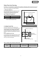
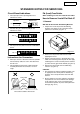
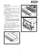
DVM-2845CI STANDARD NOTES FOR SERVICING Circuit Board Indications Pb (Lead) Free Solder 1. The output pin of the 3 pin Regulator ICs is indicated as shown. When soldering, be sure to use the Pb free solder. How to Remove / Install Flat Pack-IC Top View Out Bottom View In 1. Removal Input With Hot-Air Flat Pack-IC Desoldering Machine: 1. Prepare the hot-air flat pack-IC desoldering machine, then apply hot air to the Flat Pack-IC (about 5 to 6 seconds). (Fig. S-1-1) 2.
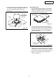
DVM-2845CI With Soldering Iron: 3. The flat pack-IC on the CBA is affixed with glue, so be careful not to break or damage the foil of each pin or the solder lands under the IC when removing it. CBA 1. Using desoldering braid, remove the solder from all pins of the flat pack-IC. When you use solder flux which is applied to all pins of the flat pack-IC, you can remove it easily. (Fig.
DVM-2845CI With Iron Wire: 2. Installation 1. Using desoldering braid, remove the solder from all pins of the flat pack-IC. When you use solder flux which is applied to all pins of the flat pack-IC, you can remove it easily. (Fig. S-1-3) 1. Using desoldering braid, remove the solder from the foil of each pin of the flat pack-IC on the CBA so you can install a replacement flat pack-IC more easily. 2. Affix the wire to a workbench or solid mounting point, as shown in Fig. S-1-5. 2.
DVM-2845CI Instructions for Handling Semiconductors Electrostatic breakdown of the semi-conductors may occur due to a potential difference caused by electrostatic charge during unpacking or repair work. 1. Ground for Human Body Be sure to wear a grounding band (1 MΩ) that is properly grounded to remove any static electricity that may be charged on the body. 2.
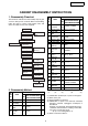
DVM-2845CI CABINET DISASSEMBLY INSTRUCTIONS 1. Disassembly Flowchart ID/ LOC. No. This flowchart indicates the disassembly steps to gain access to item(s) to be serviced. When reassembling, follow the steps in reverse order. Bend, route, and dress the cables as they were originally.
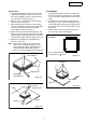
DVM-2845CI Reference Notes (L-1) CAUTION 1: Locking Tabs (L-1) are fragile. Be careful not to break them. (B) 1-1. To release eight Locking Tabs (L-1), first release five Locking Tabs (A), and then three Locking Tabs (B). (Fig. D2) (L-1) CAUTION 2: Electrostatic breakdown of the laser diode in the optical system block may occur as a potential difference caused by electrostatic charge accumulated on cloth, human body etc., during unpacking or repair work.
DVM-2845CI Screw A [5] Slide Tray Assembly Chuck arm Rotary tray washer Rotary tray spring Rotary tray washer A CN2103 (S-4) Turn [7] Power SW CBA CN2201 B (L-2) Slide Tray Assembly Short the three short lands by soldering. (Either of two places.) (L-2) Slide Tray [6] Function CBA Gear (B) Fig. D4 FPC Cable View for A Relay CBA CN5001 CN5004 FFC cable from the DVD Main CBA Unit FFC cable from the Changer CBA View for B (Relay CBA) Fig.
DVM-2845CI [14] Slide Tray Gear (B) (S-5) [8] Rear Panel (S-6) (S-12) [15] Slide Tray Gear (A) (P-1) (S-5) (S-11) (S-6) (S-5) (S-6) [17] Switch CBA Belt L (S-8) (S-6) (S-8) [13] Loading Pulley (S-13) (S-7) (S-5) [18] Tray Guide (R) (L-4) [16] Motor Assembly Fig. D6 Fig.
DVM-2845CI (S-16) [21] DVD Main CBA Unit [22] PCB Holder Fig.
DVM-2845CI SLIDE TRAY ASSEMBLY DISASSEMBLY INSTRUCTIONS 1. Disassembly Flowchart This flowchart indicates the disassembly steps to gain access to item(s) to be serviced. When Reassembly, follow the steps in reverse order. Bend, route, and dress the cables as they were originally.
DVM-2845CI Reference Notes 2. Disassembly Method 1. Disassembly note Slide the Rotary Tray slowly in the direction of the front while rotating it. 2. Reassembly note Align the rails on the Rotary Tray with the slot on the sensor and align pin A with hole A on the Rotary Tray. 3. Reassembly note Re-solder the leads on the Rotary Motor Assembly or the Detector Switch as shown in Fig. MD4. 4.
DVM-2845CI (S-1) Slide Tray [1] Chuck Arm (P-1) (W-1) (W-1) Clamper Yoke Magnet [9] Detector Switch Desolder Fig. MD1 Hole A [8] Mecha Cable Desolder Lead clamper [10] Rotary Motor Assembly [7] Gear Plate (S-8) [6] Belt L (S-6) (S-7) (S-6) 1 (S-5) [5] Plate Spring (L-1) (L-1) 2 (S-6) CN5002 Rails on the Rotary Tray [2] Rotary Tray Slot on the sensor CN5101 [8] Mecha Cable (L-1) Bottom View of the Slide Tray Pin A Fig.
DVM-2845CI CN5005 [13] Rotary Stopper Slide Tray CN5003 [15] Motion Gear Slot A Pin B Pin D (P-2) turn [12] Slot Lever Slot B (S-9) (S-9) Slot C Pin C Pin E [14] Mecha Holder Assembly Pin E [11] Relay CBA + Sensor CBA Bottom View of the Slide Tray Pin D A Slot A Pin C Slide Tray Bottom View of the Mecha Holder Assembly Short the three short lands by soldering. (Either of two places.) Hole B Cavity A Rib A FPC Cable View for A Fig.
DVM-2845CI [21] Slide Tray Chassis [20] Idler Arm [19] Idler Pad [17] Rotary Tray Gear [18] Idler Gear (P-3) [16] Loading Pulley (W-3) (W-2) (W-4) (S-10) (S-11) Fig.
DVM-2845CI TROUBLESHOOTING FLOW CHART NO.1 The power cannot be turned on. Is the fuse normal? Yes Is normal state restored when once unplugged power cord is plugged again after several seconds? Yes Is the CHG +3.3V line voltage normal? Yes Is each voltage of the secondary side normal? Yes When pressing POWER button (SW2101), is the voltage of 0V supplied to pin(42) of IC3001? Yes Is the voltage of 3.3V supplied to pin(1) of IC3001? Yes Replace IC3001. No See FLOW CHART No.2
DVM-2845CI FLOW CHART NO.6 P-ON+10V (EV+10V) is not outputted. Is 10V voltage supplied to the emitter of Q1002? No Check D1030, C1035, C1048, L1009 and the periphery circuit, and service it if defective. Yes No Is the voltage of base on Q1002 lower than the voltage of emitter on Q1002 when turning the power on? Check Q1016 and service it if defective. Yes Replace Q1002. FLOW CHART NO.7 P-ON+5V is not outputted. (P-ON+10V is outputted normally.
DVM-2845CI FLOW CHART NO.12 The fluorescent display tube does not light up. No Is 3.3V voltage supplied to Pin(13) and Pin(43) of IC2001? Yes Is the voltage of approximately -24V to -28V supplied to Pin(30) of IC2001? Yes Replace the fluorescent display tube or IC2001. Check the P-ON+3.3V line and service it if defective. No Check the -FL line and service it if defective. FLOW CHART NO.13 The key operation is not functioning.
DVM-2845CI FLOW CHART NO.14 No operation is possible from the remote control unit. Operation is possible from the DVD, but no operation is possible from the remote control unit.
DVM-2845CI FLOW CHART NO.18 [No Disc] indicated. (When the focus servo is not functioning.) Replace the DVD Main CBA Unit. No improvement can be found. Yes No Original DVD Main CBA Unit is poor. Replace the DVD Mechanism. FLOW CHART NO.19 [No Disc] indicated. (When the laser beam does not light up.) Replace the DVD Main CBA Unit. No improvement can be found. Yes No Original DVD Main CBA Unit is poor. Replace the DVD Mechanism. FLOW CHART NO.
DVM-2845CI FLOW CHART NO.21 Picture does not appear normally. Set the disc on the disc tray, and playback. Are the video signals outputted to each pin of CN1601 on the AV CBA? CN1601 CN1601 CN1601 CN1601 CN1601 1PIN 3PIN 5PIN 7PIN 9PIN No S-Y(I) Pr/Cr Pb/Cb S-Y(I/P) S-C Yes Are the video signals shown above inputted into each pin of IC1402 and IC1403? IC1402 IC1402 IC1402 IC1403 IC1403 3PIN 6PIN 8PIN 1PIN 3PIN Replace the DVD Main CBA Unit or DVD Mechanism.
DVM-2845CI FLOW CHART NO.22 Audio is not outputted. Set the disc on the disc tray, and playback. Are the analog audio signals outputted to each pin of CN1601 on AV CBA? No Replace the DVD Main CBA Unit or DVD Mechanism. CN1601 11PIN AUDIO-L CN1601 13PIN AUDIO-R Yes Are the analog audio signals inputted to each pin of IC1201. Check each line between each pin of CN1601 and each pin of IC1201 on AV CBA, and service it if defective.
DVM-2845CI FLOW CHART NO.23 Rotary tray does not function. Is the normal control voltage inputted to pins (39, 40, 41) of IC3001? For each terminal voltage, refer to FLOW CHART No.13 No Check the switches (SW2208, 2209, 2211 - 2214) and their periphery, and service it if defective. Yes No Is the voltage of 3.3V supplied to pin(1) of IC3001? Yes Is the normal control voltage outputted to pins (22, 23) of IC3001? Yes Check CHG 3.3V line and service it if detective.
M M SLED MOTOR TO SACD BLOCK DIAGRAM SPINDLE MOTOR ADAC-MD ADAC-MC TO AUDIO BLOCK DIAGRAM FS RS-232C TRAY-IN TXD RXD MECHA CBA TS PICK-UP UNIT M-MUTE AUDIO-MUTE ADAC-MD ADAC-MC ADAC-ML 2 3 JK2321 CN5007 1 2 4 5 6 CN5005 2 3 1 4 CN3001 12 9 13 14 11 RS232C-I/F INTERFACE CBA 14 13 CN201 2 3 1 4 CN301 15 14 12 11 10 CN2321 CNF02 11 4 RS232C-TX 4 12 2 RS232C-RX 2 CN3301 15 14 12 11 10 SP(+) SP(-) SL(-) SL(+) TRAY-IN DVD MAIN CBA UNIT CHANGER CBA FS(+) FS(-) TS(+) TS(-) IC2321 (
RM2 RM1 M TO SYSTEM CONTROL-1 BLOCK DIAGRAM CN401 CN1101 22 REMOTE1 SENSOR CBA UP/DOWN SW CN5002 9 8 CN3003 1 2 CHK-ON CHK-OFF GND 7 CN3001 7 5 28 AMP IC3510 (AMP) 1 TO POWER SUPPLY BLOCK DIAGRAM AV CBA TO SYSTEM CONTROL-1 BLOCK DIAGRAM CN301 5 6 7 4 1 2 CN5001 1 CHK-ON 3 CHK-OFF 4 2 4 2 JK3501 POWCON PWCHK PWSW CN1102 FP-STB FP-DIN FP-DOUT FP-CLK RS232C-TX RS232C-RX CN3001 1 3 CN5001 CN3001 8 D-SENS-A 8 6 RT-SENS-A 6 CN5001 7 RM2 5 RM1 RELAY CBA +3.
PICK-UP UNIT DETECTOR RELAY CBA CD 4 6 IC201 (SW) DVD CD-LD DVD-LD PD-MONI GND(DVD-PD) GND(CD-PD) GND(LD) 1 3 CN5004 Q253,Q254 CN201 10 CD-LD 10 AMP 8 DVD-LD 8 AMP 7 PD-MONI 7 Q251,Q252 6 GND(DVD-PD) 6 5 GND(CD-PD) 5 9 GND(LD) 9 CN5005 10 8 7 6 5 9 CN201 16 18 17 15 19 CN5004 16 18 17 15 19 SDRAM DATA(0-15) SDRAM ADDRESS(0-11) CN5005 16 18 17 15 19 C D A B CD/DVD 42 53 2 13 ~ C D A B CD/DVD SDRAM ~ 29 35 198 247 DATA RAM INST.
TO DIGITAL SIGNAL PROCESS BLOCK DIAGRAM TO AUDIO BLOCK DIAGRAM TO DIGITAL SIGNAL PROCESS BLOCK DIAGRAM TO DIGITAL SIGNAL PROCESS BLOCK DIAGRAM TO DIGITAL SIGNAL PROCESS BLOCK DIAGRAM SCK2 SPDIF PCM-DATA3 PCM-DATA2 PCM-DATA1 PCM-DATA0 PCM-LRCK PCM-BCK CLOCK-PULSE SDRAM ICF02 (SDRAM) I2C-SCL I2C-SDA YC(0-7) 2 13 31 56 74 85 1 2 F/F 5 3 ICF06 (FLIP FLOP) YC(0-7) SDRAM DATA(0-31) 16-18, 26-30 G(0-7) B(2-7)/R(0,1) 91 4-9, 12,13 YC(0-7) 50 103 191 XTAL-IN 195 CLOCK-PULSE 205 INPUT
TO VIDEO-1 BLOCK DIAGRAM VIDEO-Y(I) VIDEO-C VIDEO-Y(I/P) VIDEO-Pb/Cb VIDEO-Pr/Cr DVD MAIN CBA UNIT CN601 18 10 12 14 16 VIDEO-Y(I) VIDEO-C VIDEO-Y(I/P) VIDEO-Pb/Cb VIDEO-Pr/Cr CN1601 1 9 7 5 3 WF1 WF2 LPF LPF 4dB AMP LPF LPF 4dB AMP 6 8 LPF 4dB AMP IC1402 (VIDEO DRIVER) 4dB AMP 4dB AMP 3 1 3 IC1403 (VIDEO DRIVER) 2dB AMP 2dB AMP 2dB AMP DRIVER DRIVER DRIVER DRIVER DRIVER 2dB AMP 2dB AMP DRIVER 2dB AMP AV CBA 10 11 13 7 6 5 WF3 Y 3 1 4 JK1404 2 JK1401 S-VIDEO OUT
TO SYSTEM CONTROL-1 BLOCK DIAGRAM TO DIGITAL SIGNAL PROCESS BLOCK DIAGRAM TO SACD BLOCK DIAGRAM TO DIGITAL SIGNAL PROCESS BLOCK DIAGRAM TO SACD BLOCK DIAGRAM TO SYSTEM CONTROL-1 BLOCK DIAGRAM TO SACD BLOCK DIAGRAM ADAC-MD ADAC-ML ADAC-MC SD0/SPDIF SACD SD2 SD3 SD1 SD4 SD5 SD6 DSD-CLK DSD-MXL DSD-MXR DSD-FL DSD-FR DSD-C DSD-SW DSD-LS DSD-RS SCK1 SACD-RESET M-MUTE AUDIO-MUTE 2 1 1 2 1 2 AUDIO(L)-MUTE AUDIO(R)-MUTE SURROUND(L)-MUTE SURROUND(R)-MUTE CENTER-MUTE SUB WOOFER-MUTE 4 ICS07 (
TO DIGITAL SIGNAL PROCESS BLOCK DIAGRAM TO DIGITAL SIGNAL PROCESS BLOCK DIAGRAM TO SYSTEM CONTROL-1 BLOCK DIAGRAM CLK33M SD0/SPDIF SD1 SD2 SD3 SD4 SD5 SD6 SD7 XSAK XSHD SDCK SACD-RESET XSRQ SDEF PSP-WCK SACD-READY SACD-DATA SACD-LATCH ADAC-MD ADAC-MC SACD-RESET SACD-RESET XSRQ SDEF WCK SACD-READY SACD-DATA SACD-LATCH 169 170 171 172 173 174 175 176 167 XSAK 165 XSHD 166 SDCK 31 9 164 168 123 7 6 2 4 ADAC-MD 3 ADAC-MC DST DECODER 11 PCM-SCLK DVD MAIN CBA UNIT STREAM MANAGER DSD FADE
AC1001 AC CORD V LINE FILTER L1001 34 LATCH Q1008 F1001 1A 250V A F AV CBA SWITCHING SWITCHING CONTROL HOT Q1001 Q1003 BRIDGE RECTIFIER D1001, D1002 D1004, D1005 HOT CIRCUIT. BE CAREFUL. CAUTION ! Fixed voltage (or Auto voltage selectable) power supply circuit is used in this unit. If Main Fuse (F1001) is blown , check to see that all components in the power supply circuit are not defective before you connect the AC plug to the AC power supply.
DVM-2845CI SCHEMATIC DIAGRAMS / CBA’S AND TEST POINTS Standard Notes WARNING Many electrical and mechanical parts in this chassis have special characteristics. These characteristics often pass unnoticed and the protection afforded by them cannot necessarily be obtained by using replacement components rated for higher voltage, wattage, etc.
DVM-2845CI LIST OF CAUTION, NOTES, AND SYMBOLS USED IN THE SCHEMATIC DIAGRAMS ON THE FOLLOWING PAGES: 1. CAUTION: F A V FOR CONTINUED PROTECTION AGAINST FIRE HAZARD, REPLACE ONLY WITH THE SAME TYPE FUSE. ATTENTION: POUR UNE PROTECTION CONTINUE LES RISQES D'INCELE N'UTILISER QUE DES FUSIBLE DE MÊME TYPE. RISK OF FIRE-REPLACE FUSE AS MARKED. This symbol means fast operating fuse. Ce symbole represente un fusible a fusion rapide. 2.
DVM-2845CI DVD Main 1/8 Schematic Diagram 1 NOTE: Either IC461 or IC462 is used for DVD MAIN CBA UNIT.
DVM-2845CI DVD Main 2/8 Schematic Diagram 38
DVM-2845CI IC101 Voltage Chart ~ : Voltage is not consistent PIN.NO PLAY STOP PIN.NO PLAY STOP PIN.NO PLAY 1 3.4 3.4 33 ~ ~ 65 STOP PIN.NO PLAY STOP PIN.NO ~ ~ 97 0.1 0.1 ----- : Not used PLAY STOP PIN.NO PLAY STOP PIN.NO PLAY STOP 129 2.3 2.3 161 0 0 193 0.1 0.1 225 Unit : Volts PIN.NO PLAY 1.7 STOP 1.7 2 0 0 34 0 0 66 3.4 3.4 98 0.1 0.1 130 2.3 2.3 162 1.7 1.7 194 0.1 0.1 226 0 0 3 3.5 3.5 35 3.5 3.5 67 3.4 3.4 99 0.1 0.
DVM-2845CI DVD Main 3/8 Schematic Diagram 40
DVM-2845CI DVD Main 4/8 Schematic Diagram 41
DVM-2845CI DVD Main 5/8 Schematic Diagram 42
DVM-2845CI DVD Main 6/8 Schematic Diagram 43
DVM-2845CI DVD Main 7/8 Schematic Diagram 44
DVM-2845CI DVD Main 8/8 Schematic Diagram 45
DVM-2845CI AV 1/2 Schematic Diagram CAUTION ! Fixed voltage (or Auto voltage selectable) power supply circuit is used in this unit. If Main Fuse (F1001) is blown , check to see that all components in the power supply circuit are not defective before you connect the AC plug to the AC power supply. Otherwise it may cause some components in the power supply circuit to fail. F A V CAUTION ! For continued protection against fire hazard, replace only with the same type fuse.
DVM-2845CI AV 2/2 Schematic Diagram 47
DVM-2845CI Changer 1/2 , Function , Power Switch & Switch Schematic Diagram 48
DVM-2845CI Changer 2/2 Schematic Diagram FL2001 MATRIX CHART 7G TL./GR. TR. /CP. 6G 5G 4G PSCAN DVD A 3G 2G 1G RPT ALL CD SACD A B a h h c h h f d g b e 7G 6G 5G 4G 3G 2G 1G a a a a a a a a b b b b b b b b c c c c c c c c d d d d d d d d e e e e e e e e f f f f f f f f g g g g g g g g h TL./GR. TR./CP. i 49 DVD h RPT.
DVM-2845CI Interface Schematic Diagram 50
DVM-2845CI Relay , Sensor , Mecha & Pick Up Unit Schematic Diagram 51
DVM-2845CI WAVEFORMS 2 52
M SLED MOTOR M TS FS MECHA CBA ROTARY MOTOR PICK UP UNIT 11 2 3 DETECTOR 5 6 4 7 TRAY-IN M SPINDLE MOTOR SLIED TRAY ASSEMBLY UP/DOWN SWITCH 1 2 3 4 1 2 3 4 5 6 7 8 9 10 11 12 13 14 15 16 17 18 19 20 1 2 3 4 5 6 1 2 3 4 5 6 7 8 9 TS(+) FS(+) FS(-) TS(-) GND(CD-PD) GND(DVD-PD) PD-MONI DVD-LD GND(LD) CD-LD GND NU VREF NU B C A D CD/DVD P-ON+5V RELAY CBA CN5004 1 2 3 4 5 6 7 8 9 10 11 12 13 14 15 16 17 18 19 20 CN5005 TS(+) FS(+) FS(-) TS(-) GND(CD-PD) GND(DVD-PD) PD-MONI DVD-LD GND(LD) CD-
DVM-2845CI FIRMWARE RENEWAL MODE 5. After programming is finished, the tray opens automatically. Fig. e appears on the screen and the checksum in (*2) of Fig. e appears on the VFD. (Fig. f) 1. Turn the power on and remove the disc on the tray. 2. To put the DVD player into version up mode, press [9], [8], [7], [6], and [SEARCH MODE] buttons on the remote control unit in that order. The tray will open automatically. Fig. a appears on the screen and Fig. b appears on the VFD.
DVM-2845CI LEAD IDENTIFICATIONS 2SK3498 2SA1015-Y(TE2 F T) KRA110M-AT/P KRC110M-AT/P KTA1266-Y-AT/P KTA1267-Y-AT/P KTC3199-GR-AT/P 2SC1815-(GR)(TE2 F T) 2SA966-Y(TE6 F M) KTC3205-Y-AT/P KTA1273-Y-AT/P G D S E C B E C B 42 LD1117V UZ1086L-ADJ PT204-6B-12 M38503G4A-131FP BA6956AN 22 1 21 C 1 2 3 E KIA4558P/P RC4580IP UTC4558 CXA1511M-T4 MM1636XWRE 8 5 PST3229NR 5 1: Vin 2: Vo 3: GND 4 1: R 2: A 3: K 1 33 4 EL817(B,C) LTV-817C-F PS2561A-1(W) 23 34 22 12 44 1 16 9 1 8 1 2 3 P
DVM-2845CI EXPLODED VIEWS Cabinet 1 2L021 2L021 2L021 2L021 A16 1B1 A2 2L021 2L021 Relay CBA 2L031 2B25 C 2B3 AC1001 2L031 2L032 W3004 B 2B6 JK3501 2L011 2L011 JK1401 JK1404 C' W3003 IC1204 E' JK1202 2B1 2L051 F' G' H' D' JK1201 2L041 A AV CBA 2L103 F 2L012 2L033 E SCOTCH TAPE Changer CBA G DVD Main CBA Unit 2L012 2L033 2L012 2L033 2L011 2L011 2B1 Power SW CBA 2L041 SCOTCH TAPE 2L011 Interface CBA A21 2B11 B' D 2B7 A' 2L081 2L033 2L081 2L043 2L012 A17 A15 1L017
DVM-2845CI Cabinet 2 L1-6 B1-26 B1-41 B1-43 B1-24 B1-42 B1-3 B1-22 B1-24 B1-30 B1-30 B1-2 Mecha Holder Assembly B1-20 B1-6 B1-19 B1-21 SW5001 B1-36 B1-7 B1-37 B1-8 L1-26 B1-52 L1-5 L1-25 B1-4 B1-38 B1-9 B1-5 L1-6 Rotary Motor Assembly W5001 B1-12 B1-13 L1-11 Sensor CBA L1-23 B1-14 L1-7 Relay CBA B1-16 L1-11 Relay CBA + Sensor CBA L1-11 L1-15 L1-11 57 B1-15
DVM-2845CI PARTS LIST OF EXPLODED VIEW (CABINET1) *本表に記載されている部品は、補修用部品のため製品に使用している部品とは一部、形状、寸法などが異なる場合があります。 * The parts listed below are for maintenance only, might differ from the parts used in the unit in appearances or dimensions. * "nsp" 印の部品は常時在庫していませんので供給に長時間を要することがあります。場合によっては、供給をお断りする場合があります。 * Part indicated with the mark “nsp” are not always in stock and possibly to take a long period of time for supplying, or in some case supplying of part may be refused. Ref. No. nsp Part No.
DVM-2845CI Ref. No. nsp Part No.
DVM-2845CI PARTS LIST OF EXPLODED VIEW OF SLIDE MECHANISM UNIT (CABINET2) *本表に記載されている部品は、補修用部品のため製品に使用している部品とは一部、形状、寸法などが異なる場合があります。 * The parts listed below are for maintenance only, might differ from the parts used in the unit in appearances or dimensions. * "nsp" 印の部品は常時在庫していませんので供給に長時間を要することがあります。場合によっては、供給をお断りする場合があります。 * Part indicated with the mark “nsp” are not always in stock and possibly to take a long period of time for supplying, or in some case supplying of part may be refused. Ref. No.
Chief Ingredient of FAG-102R - Hydrocarbon synthetic oil - Lithium soap - Additives NOTE : Apply some grease to the Fill Color position.
DVM-2845CI NOTE : Apply some grease to the Fill Color position.
DVM-2845CI Packing X21 X22 X10 X5 X2 S3 S2 X4 S10 X1 S3 S2 S4 A22 Unit A30 S1 A30 63
DVM-2845CI PARTS LIST OF PACKING & ACCESSORIES *本表に記載されている部品は、補修用部品のため製品に使用している部品とは一部、形状、寸法などが異なる場合があります。 * The parts listed below are for maintenance only, might differ from the parts used in the unit in appearances or dimensions. * "nsp" 印の部品は常時在庫していませんので供給に長時間を要することがあります。場合によっては、供給をお断りする場合があります。 * Part indicated with the mark “nsp” are not always in stock and possibly to take a long period of time for supplying, or in some case supplying of part may be refused. Ref. No. nsp Part No.