Ver. 1 SERVICE MANUAL MODEL JP POA-3012CI E3 E2 EK E2A E1C E1K EUT 3 3 STEREO POWER AMPLIFIER 注 意 サービスをおこなう前に、このサービスマニュアル を必ずお読みください。本機は、火災、感電、けが などに対する安全性を確保するために、さまざまな 配慮をおこなっており、また法的には「電気用品安 全法」にもとづき、所定の許可を得て製造されてお ります。従ってサービスをおこなう際は、これらの 安全性が維持されるよう、このサービスマニュアル に記載されている注意事項を必ずお守りください。 ● For purposes of improvement, specifications and design are subject to change without notice. ● Please use this service manual with referring to the operating instructions without fail.
SAFETY PRECAUTIONS The following check should be performed for the continued protection of the customer and service technician. LEAKAGE CURRENT CHECK Before returning the unit to the customer, make sure you make either (1) a leakage current check or (2) a line to chassis resistance check. If the leakage current exceeds 0.5 milliamps, or if the resistance from chassis to either side of the power cord is less than 460 kohms, the unit is defective.
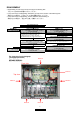
注 意 サービス、点検時にはつぎのことにご注意願います。 ◎注意事項をお守りください! ◎サービス後は安全点検を! サービスのとき特に注意を必要とする個所については キャビネット、部品、シャーシなどにラベルや捺印で注意 事項を表示しています。これらの注意書きおよび取扱説明 書などの注意事項を必ずお守りください。 サービスのために取り外したねじ、部品、配線などが元ど おりになっているか、またサービスした個所の周辺を劣化 させてしまったところがないかなどを点検し、外部金属端 子部と、電源プラグの刃の間の絶縁チェックをおこなうな ど、安全性が確保されていることを確認してください。 ◎感電に注意! (1) このセットは、交流電圧が印加されていますので通電 時に内部金属部に触れると感電することがあります。 従って通電サービス時には、絶縁トランスの使用や手 袋の着用、部品交換には、電源プラグを抜くなどして 感電にご注意ください。 (2) 内部には高電圧の部分がありますので、通電時の取扱 には十分ご注意ください。 (絶縁チェックの方法) 電源コンセントから電源プラグを抜き、アンテナやプラグ などを外し、電源
DIMENSION 25.5 max W434 X H171 X D410 372 12.5 54.5 244.
WIRE ARRANGEMENT ワイヤー整形図 If wire bundles are untied or moved to perform adjustment or parts replacement etc., be sure to rearrange them neatly as they were originally bundled or placed afterward. Otherwise, incorrect arrangement can be a cause of noise generation.
CAUTION IN SERVICING サービス時の注意事項 Initializing POA-3012CI 本機の初期化について S-81/S-81DAB initialization should be performed when the ucom and peripheral parts of ucom are replaced. マイコンやマイコン周辺部品を交換した場合は、本機の初 期化をおこなってください。 1. Unplug the power cord from the power outlet. 1. 電源コードをコンセントから抜きます。 2. Connect the power cord to the power outlet while simultaneously pressing the ZONE 5 and DISPLAY buttons. 2. " ZONE 5 " ボタンと "DISPLAY" ボタンを同時に押しなが ら、電源コードをコンセントへ接続します。 3.
DISASSEMBLY • Disassemble in order of the arrow of the figure of following flow. 下記フロー図の矢印の順番にはずしてください。 • In the case of the re-assembling, assemble it in order of the reverse of the following flow. 再組み立ての場合は、下記のフローの逆の順番に組立ててください • In the case of the re-assembling, observe "attention of assembling" it. 再組み立ての場合は、「組立のご注意」を遵守してください。 TOP COVER SUB ASSY REAR PANEL FRONT PANEL SUB ASSY ETHERNET UNIT Refer to "EXPLOTED VIEW" Refer to "DISASSEMBLY 1.FRNOT PANEL SUB ASSY" Refer to "DISASSEMBLY 4.
1. FRONT PANEL SUB ASSY proceeding ( 手順 ) : TOP COVER SUB ASSY → FRONT PANEL SUB ASSY (1) Remove the screws. ( ねじをはずす。) Bottom view CX121 Picture B (2) Disconnect the connector wire and FFC Cables. (コネクターワイヤーと FFC ケーブルをはずす。 ) FFC CABLE Picture B ETHERNET UNIT CX932 CX931 Picture F Please refer to "EXPLODED VIEW " for the disassembly method of each P.W.B included in FRNOT PANEL SUB ASSY.
2. POWER SUPPLY UNIT proceeding ( 手順 ) : TOP COVER SUB ASSY → → FRONT PANEL SUB ASSY POWER SUPPLY UNIT (1) Loose the cord holders. ( コードホルダーをゆるめる。) POWER SUPPLY UNIT Picture A Cord holder : Loose Cord holder : Loose (2) Disconnect the connector wires.(コネクターワイヤーをはずす。) POWER SUPPLY UNIT CX062 CX023 CX022 CX021 CX058 CX032 CX031 Picture A CX041 CX936 CX935 CX933 CX934 CX938 CX937 (3) Remove the screws.
(4) POWER SUPPLY UNIT board off the PCB HOLDER.( PCB HOLDER から POWER SUPPLY UNIT 基板をはずす。) PCB HOLDER : Disconnect Picture A POWER SUPPLY UNIT 3. SUB TRANS proceeding ( 手順 ) : TOP COVER SUB ASSY → FRONT PANEL SUB ASSY → POWER SUPPLY UNIT → SUB TRANS (1) Remove the screws.
4. ETHERNET UNIT proceeding ( 手順 ) : TOP COVER SUB ASSY → ETHERNET UNIT (1) Disconnect the connector wires and FFC Cables.(コネクタワイヤーと FFC ケーブルをはずす。 ) FFC CABLE FFC CABLE CY039 Picture C CY062 (2) Loose the FFC Holder.( FFC ホルダーをゆるめる 。) FFC HOLDER : Loose ETHERNET UNIT Picture E POWER AMP UNIT (3) Remove the screws.
Picture B (4) Disconnect the EHTHERNET UNIT.(ETHERNET UNIT をはずす。 ) Picture B ETHERNET UNIT 5. AUDIO SIGNAL UNIT & INPUT UNIT proceeding ( 手順 ) : TOP COVER SUB ASSY → AUDIO SIGNAL UNIT & INPUT UNIT (1) Disconnect the connector wire and FFC Cables, and remove the screw.
(2) AUDIO SIGNAL UNIT board off the INPUT UNIT.(AUDIO UNIT を INPUT UNIT からはずす。) PCB HOLDER AUDIO SIGNAL UNIT Picture B INPUT UNIT 6. POWER AMP UNIT (6 units). proceeding ( 手順 ) : TOP COVER SUB ASSY → POWER AMP UNIT (6 units) (1) Remove the screws and disconnect the connector wires.
7. REAR PANEL proceeding ( 手順 ) : TOP COVER SUB ASSY → REAR PANEL Please refer to "EXPLODED VIEW " for the disassembly method of REAR PANEL. REAR PANEL のはずしかたは "EXPLODED VIEW " を参照してください。 8. POWER TRANS proceeding ( 手順 ) : TOP COVER SUB ASSY → → FRONT PANEL SUB ASSY POWER TRANS Please refer to "EXPLODED VIEW " for the disassembly method of POWER TRANS.
SPECIAL MODE No. 1 特殊モード Function ZONE LED Display No. Version display 1 動作 バージョン表示 • Connect the power cord to the power outlet while simultaneously pressing the ZONE 6 and MENU buttons. • The item number is displayed replay from q to u each time the DISPLAY button is pressed. ・ 本体 ZONE 6 ボタンと MENU ボタンを同時に押しながら AC コードを接続する。 DISPLAY ボタンを押すとごとに q から u の表示を繰り返す。 q Serial No q Serial No S e r i a l N o . e DM850 Version V e r .
No. 5 Function ZONE LED Display No. Installer initialization mode 5 z Only the data for Installer setup is initialized Installer mode 6 ・ Connect the power cord to the power outlet while simultaneously pressing the ZONE 4 and SETUP buttons. 7 When failing in rewriting to Main Microprocessor ROM, it's rewritten in DPMS compulsorily.
TROUBLE SHOOTING トラブルシューティング FLOW CHART NO.1 フローチャート NO.1 The power cannot be turned on. (Power indication LED dose not light) 電源が入らない。(電源表示LEDが点灯しない) NO Is the voltage of 6V supplied to C147? YES NO Is the voltage of 4V supplied to C150? Disconnection of T101 or trouble of D101-104. NO T101の断線またはD101-104の故障 はい いいえ C150に4Vの電圧が供給されているか? Trouble of IC104. IC104の故障 はい YES Is the voltage of Hi (3.
BLOCK/LEVEL DIAGRAM 0dB BUFFER H.P.F 80Hz 12dB/oct INPUT SELECT ELECTORIC VOLUME Power Amp Odd CH -25.0dB Even CH 25.0dB Odd CH ONLY 4052 ELECTRIC VOLUME −∞㨪+4.0dB LCH 4053 + BUS INPUT dB + Even ch SPEAKER RELAY POWER AMP PRE-AMP DA428440-30 0dB SPEAKER OUT RCH + + LCH CASCADE OUT RCH TC94A32 12V TRIGGER 4053 0dB ±5V ±12V + ±30V AUDIO SIGNAL SENSE L/R/L+R/AUX/H.P.F/ BRIDGE AUX COMMUNICATION (BCOIC-DM850-QCL/ RTL8201CP) RS232C Ethernet − CONTROL (u-com) RS232C/Ethernet P.
SEMICONDUCTORS Only major semiconductors are shown, general semiconductors etc. are omitted to list. 主な半導体を記載しています。汎用の半導体は記載を省略しています。 1.
BCOIC-DM850-CQL Functional Diagram 20 POA-3012CI
P13/D11 P14/D12 P15/D13/INT3 P16/D14/INT4 P17/D15/INT5 P20/AN20/A0(/D0/-) P21/AN21/A1(/D1/D0) P22/AN22/A2(/D2/D1) P23/AN23/A3(/D3/D2) P24/AN24/A4(/D4/D3) P25/AN25/A5(/D5/D4) P26/AN26/A6(/D6/D5) P27/AN27/A7(/D7/D6) VSS P30/A8(/-/D7) VCC2 P31/A9 P32/A10 P33/A11 P34/A12 P35/A13 P36/A14 P37/A15 P40/A16 P41/A17 M3062LFGPGP (IC701) 75 74 73 72 71 70 69 68 67 66 65 64 63 62 61 60 59 58 57 56 55 54 53 52 51 P12/D10 P11/D9 P10/D8 P07/AN07/D7 P06/AN06/D6 P05/AN05/D5 P04/AN04/D4 P03/AN03/D3 P02/AN02/D2 P01/AN01/D1
Terminl Function PIN No.
PIN No. PIN Name Port Name Function I/O Remarks 61 P3_0/A8(/D7) CH1 Channel switching 62 VSS VSS2 VSS O I 63 P2_7/ANA2_7(/D7/D6) T.THERMO T.THERMO SW I Error : "H" 64 P2_6/ANA2_6(/D6/D5) TEMP Temperature detect I Error : "H" 65 P2_5/ANA2_5(/D5/D4) INPUT_B 66 P2_4/ANA2_4(/D4/D3) INPUT_A O 67 P2_3/ANA2_3(/D3/D2) BTL O O O 68 P2_2/ANA2_2(/D2/D1) H.P.F 69 P2_1/ANA2_1(/D1/D0) SIGNAL SENS I 70 P2_0/ANA2_0(/D0/-) ENA O signal : "L" 71 P1_7/D15/INT5 TRG.
DA428440E-E (IC501) BLOCK DIAGRAM Control chip OCM 6 Current Prot / HF Prot 25 ZB1 23 FB1 VDCK 10 VSCK 8 DCG 7 32 PWMFB1 Voltage check Driver chip1 Level shift ENA 4 TEST 19 Inverting IN1- 17 AGND1- 16 Non-inverting IN2+ 15 AGND2+ 14 28 VD1 High drive Current detect Rec. Soft Limit COM/MECC Control ch1 Rec.
Terminl Function Pin No. Pin Name 1 2 3 AGND VSS THM 4 ENA 5 6 NC OCM 7 DCG 8 VSCK 9 10 AGND VDCK 11 12 13 14 VSS AGND NC AGND2 15 IN2+ 16 AGND1 17 IN1- 18 19 20 21 22 23 24 25 NC TEST VSS AGND VDD FB1 NC ZB1 26 27 28 29 30 31 32 33 34 35 36 37 38 39 40 41 42 VDR1 VD1 VD1 VS1 VS1 PWM1 PWMFB1 SUB VS VDR2 VD2 VD2 VS2 VS2 PWM2 PWMFB2 ZB2 43 44 NC FB2 Function Analog ground for control chip power supply. Negative power supply for control chip (-5V).
TC94A32F (IC232, 238, 244, 250, 256, 262) CD4508BPWR (IC421~426) RESET A STROBE A DUTPUT DISABLE A D0 A Q0 A D1 A Q1 A D2 A Q2 A D3 A Q3 A Vss 1 2 3 4 5 6 7 8 9 10 11 12 24 23 22 21 20 19 18 17 16 15 14 13 FUNCTIONAL DIAGRAM OUTPUT DISABLE D0A D1A D2A D3A STROBE RESET OUTPUT DISABLE D0B D1B D2B D3B VDD Q3 B D3 B Q2 B D2 B Q1 B D1 B Q0 B D0 B OUTPUT DISABLE B STROBE B RESET B 4-BIT LATCH 3-STATE OUTPUTS 4-BIT LATCH 3-STATE OUTPUTS STROBE RESET HIN202EIBNZ-T (IC801) +5V 16 0.
BU4052BCF (IC202, 204, 206, 208, 210, 212, 214, 216, 218, 220, 222, 224) Y0 1 Y2 2 Y0 Y2 Y OUT / IN COMMON 3 Y Y3 4 Y3 Y1 5 Y1 X2 X1 INH 6 VEE VEE 7 A VSS 8 TC74HC00AF (IC409~411) 1A 1 Y1 1 15 X2 Y0 2 Z1 3 Z 13 COMMON X X3 B 16 VDD 14 X1 X OUT / IN X0 INH BU4053CF (IC231, 237, 243, 249, 255, 261) 14 VCC 4 12 X0 Z0 5 11 X3 INH 6 10 A VEE 7 9 B VSS 8 TC74VHCT08AFT (IC703, 912) 1A 1 16 VDD 15 Y Y1 Y0 Y Z1 X Z X1 Z0 X0 INH VEE A C B 14 X 13 X1 12 X0 11 A 10 B 9 C T
NJM5532MD (IC225, 226) NJM2068MD-TE1 (IC201, 203, 205, 207, 209, 211, 213, 215, 217, 219,221, 223, 233~236, 239~242, 245~248, 251~254, 257~260, 263 ~266) NJM2831F (IC104) 5 1 4 2 1. CONTROL 2. GND 3. NC 4. VOUT 5. VIN 3 VIN VOUT Control Thermal Protection Bandgap Reference GND PQ070XZ01ZP (IC907) PQ1CG41H2FZ (IC101) 1 2 3 4 1 2 3 4 5 2 1 NJM7905FA(S) (IC108) NJM7912FA(S) (IC106) FRONT VIEW FRONT VIEW GND Input Output 1: Vcc 2: N.C.
TRANSISTORS KTA1268BL KTC3200BL 2SC4793 (Y) 2SK373 (Y) FRONT VIEW FRONT VIEW FRONT VIEW 2SB1412 2SA1037K(S/R) 2SC2412K(S) 2SD2114K 2SC4672 2 1 (1) (2) (3) ECB SGD B CE DTA114EK NPN Type B 2 1 R1 DTA114EK C 10kohm 10kohm 10kohm 6 3 4 22kohm DTC143EK 4.7kohm 4.
2.
ANODE CONNECTION 31 POA-3012CI
---MEMO--- 32 POA-3012CI
PRINTED WIRING BOARDS 1U-3868 POWER AMP P.W.B.
1U-3869 ETHERNET P.W.B.
1U-3870 INPUT P.W.B.
1U-3870 INPUT P.W.B.
1U-3871 MICON/FLD P.W.B.
1U-3871 MICON/FLD P.W.B.
NOTE FOR PARTS LIST 部品表について • • Parts for which "nsp" is indicated on this table cannot be supplied. When ordering of part, clearly indicate "1" and "I" (i) to avoid missupplying. • Ordering part without stating its part number can not be supplied. • Part indicated with the mark " ★ " is not illustrated in the exploded view. • Not including General-purpose Carbon Film Resistor in the P.W.Board parts list. (Refer to the Schematic Diagram for those parts.
PARTS LIST OF P.W.B. UNIT * 本表に "nsp" と記載されている部品は供給できません。 * Parts for which "nsp" is indicated on this table cannot be supplied.\ * 本表に記載されている部品は、補修用部品のため製品に使用している部品とは一部、形状、寸法などが異なる場合があります。 * The parts listed below are for maintenance only, might differ from the parts used in the unit in appearances or dimensions. Note: The symbols in the column "Remarks" indicate the following destinations. E3: U.S.A. & Canada model E2: Europe model 1U-3868 POWER AMP P.W.B. UNIT ASS'Y (E3 model) 1U-3868B POWER AMP P.W.B.
Ref. No. Part No. Part Name C545-550 00D2571022900 CK73B2A104KT-3216 C551,552 00D2568038004 CF99--2EAC104M C553,554 00D2546278006 CE68W1==902M(DL) C555 00D2544410921 CE04W1H100MT(KMG) C556 00D2545027902 CA04H1C101MT(SA) Remarks Q'ty New * OTHERS PARTS GROUP CX031 nsp 3P VH CONNECTOR BASE CX151 nsp 15P KR CON BASE(L) z F501,502 00D2061046001 FUSE 6.3AUL 20MM for E3 z F501,502 00D2061036011 FUSE (6.
1U-3869 ETHERNET P.W.B. UNIT ASS'Y (This P.W.B. UNIT ASSY is replaced by Assy level.) Ref. No. Part No.
Ref. No. Part No.
Ref. No. Part No. Part Name FB401 nsp E.FIL(BLM21PG221SN1)+2125 FB801-808 nsp E.FIL(BLM21PG221SN1)+2125 FB901,902 nsp CHIP EMIFIL(11A121) +1608 FB904-906 nsp CHIP EMIFIL(11A121) +1608 FB908 nsp CHIP EMIFIL(11A121) +1608 JK213 nsp YKC21-4086V 2L4P FS BK AU JK401 nsp 2P MINI JACK JK801 nsp 9P D-SUB CONNECTOR JK901 nsp 8P MODULAR X901 nsp FCX-03(24.
1U-3870 INPUT P.W.B. UNIT ASS'Y Ref. No. Part No.
Ref. No. Part No. Part Name D401-418 00D2760794900 KDS160-RTK/P D421-444 00D2760794900 KDS160-RTK/P ZD201-228 00D2760798951 UDZS4.
Ref. No. Part No.
Ref. No. C348 C349,350 Part No.
Ref. No. Part No. C482 nsp C483 00D2544661987 C484-486 nsp Part Name Remarks Q'ty New CF73=1C104JT(ECHUB5)+3225 CE67C1H010MT(RV2) CK73B1H102KT +1608 OTHERS PARTS GROUP CW072 00D2042692115 7P SCN-SCN CON.
1U-3871 MICON/FLD P.W.B. UNIT ASS'Y (E3 model) 1U-3871B MICON/FLD P.W.B. UNIT ASS'Y (E2 model) Ref. No. Part No.
Ref. No. FL701 Part No.
Ref. No. Part No.
Ref. No. FH101-109 Part No.
AC INLET P.W.B. UNIT ASS'Y (E3 Only) Ref. No. Part No. Part Name Remarks Q'ty New CAPACITORS GROUP C101,102 00D2538029700 CK45F2EAC222MC (KX) OTHERS PARTS GROUP W103 nsp 1P CONTACT ASS * nsp 2P CORD ASSY * nsp UL TUBE(12.
---MEMO--- 55 POA-3012CI
EXPLODED VIEW 110 37 102 105 115 115 115 102 1-4 WARNING: Parts marked with this symbol have critical characteristics. Use ONLY replacement parts recommended by the manufacturer.
PARTS LIST OF EXPLODED VIEW * 本表に "nsp" と記載されている部品は供給できません。 * Parts for which "nsp" is indicated on this table cannot be supplied. * 本表に "nsp" と記載されている基板 ASS’Y は供給できません。基板 ASS’Y の修理の際には基板部品表を確認のうえ、交換部品を発注してください。 * P.W.B. ASS'Y for which "nsp" is indicated on this table cannot be supplied. When repairing the P.W.B. ASS'Y, check the board parts table and order replacement parts.
Ref. No. Part No. Part Name Remarks Q'ty New 35 nsp SHIELD SHEET 1 * 36 nsp PUSH RIVET NRP242 4 * 37 nsp UL TUBE (12.7)BK 1 38 nsp SHIELD BRACKET 6 * 39 nsp INSULATING SHEET 6 * 40 nsp SHIELD COVER 6 * 41 nsp GND PLATE 6 * 42 nsp INSULATING SHEET 6 * 43 nsp SHIELD PLATE AMP1 6 * 44 nsp SHIELD PLATE 6 * 45 nsp INSULATING AMP1 6 * 46 nsp INSULATING AMP2 6 * 47 00DGEN8688 TOP COVER SUB ASSY 1 48 nsp EMIGASKET RFSG070100 49 nsp SERIAL NO.
Ref. No. Part No. Part Name Remarks Q'ty 109 0RD4738064000 4X8 CBTS (B)-B-3P for E3 (Serial No. 1~330) 8 109 0RD4770263005 3P SWELLING SCREW for E3 (Serial No. 331~) 8 109 0RD4770263005 3P SWELLING SCREW for E2 8 110 0RD4700009022 3X6 CPS (SW.W) ZNP for E2 3 110 0RD4700009022 3X6 CPS (SW.
PACKING VIEW 208 213 202 203 204 201 206 205 205 207 202 PARTS LIST OF PACKING & ACCESSORIES * 本表に "nsp" と記載されている部品は供給できません。 * Parts for which "nsp" is indicated on this table cannot be supplied. * 本表に記載されている部品は、補修用部品のため製品に使用している部品とは一部、形状、寸法などが異なる場合があります。 * The parts listed below are for maintenance only, might differ from the parts used in the unit in appearances or dimensions. Note: The symbols in the column "Remarks" indicate the following destinations. E3 : U.S.A.
WIRING DIAGRAM 61 POA-3012CI
NOTE FOR SCHEMATIC DIAGRAM WARNING: Parts marked with this symbol z have critical characteristics. Use ONLY replacement parts recommended by the manufacturer. 配線図について z 印の部品は安全を維持するために重要な部品です。 従って交換時は必ず指定の部品を使用してください。 注) CAUTION: (1) 指定なき抵抗値は Ω、k は kΩ、M は MΩ を示す。 Before returning the unit to the customer, make sure you make either (1) a leakage current check or (2) a line to chassis resistance check. If the leakage current exceeds 0.
1 2 3 4 5 6 7 8 A B C D E SIGNAL LINE SCHEMATIC DIAGRAMS (1/9) 1U-3868-1 1U-3868-2 POWER AMP UNIT FFC GUIDE POA-3012CI F
1 2 3 4 5 6 7 8 A B C D E SIGNAL LINE SCHEMATIC DIAGRAMS (2/9) 1U-3869-1 COMMUNICATION UNIT(1/2) POA-3012CI F
1 2 3 4 5 6 7 8 A B C D E SCHEMATIC DIAGRAMS (3/9) 1U-3869-1 COMMUNICATION UNIT(2/2) POA-3012CI F
1 2 3 4 5 6 7 8 A B C D E SIGNAL LINE SCHEMATIC DIAGRAMS (4/9) 1U-3870-1 INPUT UNIT(1/2) POA-3012CI F
1 2 3 4 5 6 7 8 A B C D E SCHEMATIC DIAGRAMS (5/9) 1U-3870-1 INPUT UNIT(2/2) POA-3012CI F
1 2 3 4 5 6 7 8 A B C D E SIGNAL LINE SCHEMATIC DIAGRAMS (6/9) 1U-3870-2 SIGNAL CONTROL UNIT(1/2) POA-3012CI F
1 2 3 4 5 6 7 8 A B C D E SIGNAL LINE SCHEMATIC DIAGRAMS (7/9) 1U-3870-2 SIGNAL CONTROL UNIT(2/2) POA-3012CI F
1 2 3 4 5 6 7 8 A B C D E SCHEMATIC DIAGRAMS (8/9) 1U-3871-1 1U-3871-2 1U-3871-3 M-CON UNIT ENCODER UNIT P.
1 2 3 4 5 6 7 8 A B C D E SCHEMATIC DIAGRAMS (9/9) 1U-3871-4 1U-3871-5 P.