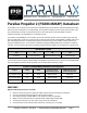
www.parallax.com/P2 ⬝ sales@parallax.com ⬝ support@parallax.com ⬝ +1 888-512-1024 Parallax Propeller 2 (P2X8C4M64P) Datasheet The Propeller 2 is a multicore microcontroller for embedded systems that delivers high-speed parallel processing with low current consumption in a small package.
● ● ● ● ● ● ● ● ● ● 6-clock custom-bytecode executor for interpreted languages Ability to stream Hub RAM and/or Lookup RAM to DACs and pins or HDMI modulator Ability to stream pins and/or ADCs to Hub RAM Live colorspace conversion using a 3 x 3 matrix with 8-bit signed/unsigned coefficients Pixel blending instructions for 8:8:8:8 data 16 unique event trackers that can be polled and waited upon 3 prioritized interrupts that trigger on selectable events Hidden debug interrupt for single-stepping, breakpoint,
● ● ● ● ● ● ● Programmable 32-bit clock output, transition output, NCO/duty output Triangle/sawtooth/SMPS PWM output, 16-bit frame with 16-bit prescaler Quadrature decoding with 32-bit counter, both position and velocity modes 16 different 32-bit measurements involving one or two signals USB full-speed and low-speed (via odd/even pin pairs) Synchronous serial transmit and receive, 1 to 32 bits, up to clock/2 baud rate Asynchronous serial transmit and receive, 1 to 32 bits, up to clock/3 baud rate Six cloc
Cog RAM 11 Register RAM 11 Lookup RAM 12 Execution 13 Starting And Stopping Cogs 14 Hub 14 Hub RAM 14 Cog-to-Hub RAM Interface 14 System Clock 16 Locks 17 CORDIC Solver 18 Smart I/O Pins 19 Pin Modes 19 I/O Pin Circuit 23 Equivalent Schematics for Each Unique I/O Pin Configuration 24 Smart Modes 30 PROPELLER 2 ASSEMBLY LANGUAGE (PASM2) IN BRIEF 33 Math and Logic Instructions 33 Pin & Smart Pin Instructions 36 Branch Instructions 37 Hub Control, FIFO, & RAM Instruction
PACKAGING 46 CHANGE LOG 47 PARALLAX INCORPORATED 47 Additional Documentation and Resources For additional documentation and resources, including programming tools, visit www.parallax.com/P2. The latest version of this datasheet, along with links to a commentable Google Doc version, are available from the Documentation section. In addition, there are links to more in-depth references for the Propeller 2 and its Spin2 and PASM2 languages, which may include commentable Google Docs.
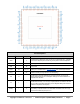
Pin Descriptions Pin Name Direction V (typ) Description GND - 0 Exposed Pad (underside of chip); ground for core and smart pins – internally connected to exposed pad. Connect to ground plane for thermal dissipation. TEST I 0 Tied to ground VDD - 1.8 P0-63 I/O 0 to 3.3 Vxxyy - 3.3 XO O - Crystal Output. Provides feedback for an external crystal, or may be left disconnected depending on CLK Register settings. No external resistors or capacitors are required. Core power Smart pins.
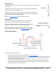
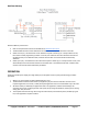
Hardware Connections Minimal Connections The Propeller 2 is programmed via four wires and may optionally include an external crystal, reset switch, SPI Flash and/or microSD memory. Minimal Propeller 2 Connections ● ● ● ● ● ● ● ● All VDD pins must be connected to a single 1.8 V supply. All Vxxyy pins must be connected to 3.3 V. The Vxxyy pins can share a common 3.3 V supply, or be split across multiple supplies.
External Crystal The internal clock reference is good for very low power applications, but is also fairly low accuracy. For applications that require higher accuracy (ex: handling high speed data) an external clock source is connected to XI/XO. Typically a crystal would be connected between XI and XO, but an external clock source could also be connected to XI only, with common options including a clock source generator, oscillator, or MEMS resonator.
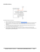
MicroSD Boot Memory MicroSD Boot Memory Connections ● ● ● ● Refer to all requirements and recommendations for Minimal Connections When the Propeller 2 starts up (or is reset) with this circuit, it will automatically boot from firmware saved on the microSD card. If microSD boot fails, a further serial window of 60 seconds will be followed by shutdown. The microSD card must be formatted as FAT32, and the boot firmware file must be saved in the root of the microSD card with the special filename: _P2_BOOT.
Dual Boot Memory Dual Boot Memory Connections ● ● ● ● Refer to all requirements and recommendations for Minimal Connections The Boot Mode Selection switch determines the active boot device; either SPI Flash or microSD. Switch closed (on) = SPI Flash boot mode : When the Propeller 2 starts up (or is reset) with this circuit, there will be a serial programming window of 100 ms, then automatic boot from firmware stored in the SPI flash memory.
SYSTEM ORGANIZATION The Propeller 2 includes the following subsystems.
Dual-purpose Registers RAM registers $1F0 through $1F7 may either be used as general-purpose registers, or may be used as special-purpose registers if their associated functions are enabled.
through their Lookup RAMs. Use the SETLUTS instruction to enable/disable this feature and SETSE1..4 to facilitate handshaking if necessary. Note that this adjacent cog access is implemented on the Lookup RAM's 2nd port, which is also used by the streamer in DDS/LUT modes; these are not intended to used simultaneously. Execution Cogs employ a five-stage pipelined execution architecture. When the execution pipeline is full, each PASM2 instruction effectively takes as little as two clock cycles to execute.
Starting And Stopping Cogs Any cog can start or stop any other cog, or restart or stop itself. Each cog has a unique ID which can be used to start or stop it. It's also possible to start free (stopped or never started) cogs, without needing to know their IDs. This way, applications can simply start free cogs, as needed, and as those cogs retire by stopping themselves or getting stopped by others, they return to the pool of free cogs to become available again for restarting.
Cogs can access Hub RAM either via the sequential FIFO interface, or by waiting for RAM slices of interest, while yielding to the FIFO. If the FIFO is not busy (which is soon the case if data is not being read from or written to it) random accesses will have full opportunity to access the composite Hub RAM. There are three ways the hub FIFO interface can be used, and it can only be used for one of these at a time: ● ● ● Hub execution (when the PC is $00400..
System Clock The system clock is the time base for all internal components and can be configured in several ways.
%SS Clock Source Notes %11 PLL CC != %00 and E=1, allow 10ms for crystal+PLL to stabilize before switching to PLL %10 XI CC != %00, allow 5ms for crystal to stabilize before switching to XI pin %01 RCSLOW ~20 kHz, can be switched to at any time, low-power %00 RCFAST 20 MHz+, can be switched to at any time, used on boot-up. WARNING: Incorrectly switching away from the PLL setting (%SS = %11) can cause a glitch which will hang the clock circuit.
allowing one cog at a time the exclusive status of 'owner' of a particular lock ID. In order to be useful, all participant cogs must agree on a lock's ID and what purpose it serves. The LOCK instructions are: LOCKNEW D {WC} LOCKRET {#}D LOCKTRY {#}D {WC} LOCKREL {#}D {WC} Lock Usage In order to use a lock, one cog must first allocate a lock with LOCKNEW and communicate that lock's ID with other cooperative cogs.
Square Root Use the QSQRT instruction on a 64-bit number and retrieve the square root CORDIC result with the GETQX instruction. (X, Y) Rotation Use the SETQ instruction followed by the QROTATE instruction to rotate a 32-bit signed Y and X point pair by an unsigned 32-bit angle and retrieve the CORDIC results with the GETQX and GETQY instructions for X and Y, respectively.
PINA or PINB Input Selector %AAAA %BBBB Selection 0xxx true (default) 1xxx inverted x000 this pin's read state (default) x001 relative +1 pin's read state x010 relative +2 pin's read state x011 relative +3 pin's read state x100 this pin's OUT bit from cogs x101 relative -3 pin's read state x110 relative -2 pin's read state x111 relative -1 pin's read state PINA and PINB Logic/Filtering %FFF Logic/Filter 000 A, B (default) 001 A AND B, B 010 A OR B, B 011 A XOR B, B 100 A, B,
The Pin Modes corresponding to the 13-bit M field are described by this table. Copyright © Parallax Inc.
Pin DIR/OUT Control (%TT) Default = %00 for odd pins 'OTHER' = even pin's NOT output state (diff source) for even pins 'OTHER' = unique pseudo-random bit (noise source) for all pins 'SMART' = smart pin output which overrides OUT/OTHER 'DAC_MODE' is enabled when P[12:10] = %101 'BIT_DAC' outputs {2{P[7:4]}} for 'high' or {2{P[3:0]}} for 'low' in DAC_MODE for smart pin mode off (%MMMMM = %00000) DIR enables output for non-DAC_MODE 0x OUT drives output 1x OTHER drives output for DAC_MODE 00 OUT enab
I/O Pin Circuit Below is a diagram of a single I/O pin circuit which is powered from its local 3.3V supply pin (Vxxyy). It connects to its own physical pin (PINA), as well as its adjacent odd or even pin (PINB). I/O Pins P0 and P1 see each other as adjacent pins, as do P2 and P3, etc. Copyright © Parallax Inc.
Equivalent Schematics for Each Unique I/O Pin Configuration Copyright © Parallax Inc.
Copyright © Parallax Inc.
Copyright © Parallax Inc.
Copyright © Parallax Inc.
Copyright © Parallax Inc.
Copyright © Parallax Inc.
Smart Modes Each I/O pin has built-in 'smart pin' circuitry which, when enabled, performs an autonomous function on the pin. Smart pins free the cogs from the need to micromanage many I/O operations by providing high-bandwidth concurrent hardware functions that cogs could otherwise not perform as well through I/O pin manipulating instructions.
any number of cogs can read a smart pin simultaneously without bus conflict by using RQPIN ('read quiet'), since it does not utilize the smart pin input bus for acknowledgement signalling (like RDPIN does). Each smart pin writes to it's output bus to convey its Z result and a special flag. The RDPIN and RQPIN multiplex and read these buses, so that a pin's Z result is read into D and its special flag can be read into C. C will be either a mode-related flag or the MSB of the Z result.
1 10000 time A-states 10001 time A-highs 10010 time X A-highs/rises/edges -or- timeout on X A-high/rise/edge 10011 for X periods, count time 10100 for X periods, count states 10101 for periods in X+ clocks, count time 10110 for periods in X+ clocks, count states 10111 for periods in X+ clocks, count periods 11000 ADC sample/filter/capture, internally clocked 11001 ADC sample/filter/capture, externally clocked 11010 ADC scope with trigger 110111 USB host/device even/odd pin pair = DM
PROPELLER 2 ASSEMBLY LANGUAGE (PASM2) IN BRIEF Math and Logic Instructions Instruction Description Clocks Reg, LUT, & Hub ABS D {WC/WZ/WCZ} Get absolute value of D into D. D = ABS(D). C = D[31]. * 2 ABS D,{#}S {WC/WZ/WCZ} Get absolute value of S into D. D = ABS(S). C = S[31]. * 2 ADD D,{#}S {WC/WZ/WCZ} Add S into D. D = D + S. C = carry of (D + S). * 2 ADDS D,{#}S {WC/WZ/WCZ} Add S into D, signed. D = D + S. C = correct sign of (D + S).
LOC PA/PB/PTRA/PTRB,#{\}A Get {12'b0, address[19:0]} into PA/PB/PTRA/PTRB (per W). If R = 1, address = PC + A, else address = A. "\" forces R = 0. 2 MERGEB D Merge bits of bytes in D. D = {D[31], D[23], D[15], D[7], ...D[24], D[16], D[8], D[0]}. 2 MERGEW D Merge bits of words in D. D = {D[31], D[15], D[30], D[14], ...D[17], D[1], D[16], D[0]}. 2 MODC c Modify C according to cccc. C = cccc[{C,Z}]. 2 MODCZ c,z Modify C and Z according to cccc and zzzz. C = cccc[{C,Z}], Z = zzzz[{C,Z}].
D[31]. * Shift arithmetic right. D = [31:0] of ({{32{D[31]}}, D[31:0]} >> S[4:0]). C = last bit shifted out if S[4:0] > 0, else D[0]. * 2 {WZ} Next instruction's S value = unsigned (D[15:0] * S[15:0]) >> 16. * 2 {WZ} SAR D,{#}S {WC/WZ/WCZ} SCA D,{#}S SCAS D,{#}S Next instruction's S value = signed (D[15:0] * S[15:0]) >> 14. In this scheme, $4000 = 1.0 and $C000 = -1.0. * 2 SETBYTE {#}S Set S[7:0] into byte established by prior ALTSB instruction.
Pin & Smart Pin Instructions Instruction Description Clocks Cog, LUT & Hub Pin DIRC {#}D {WCZ} DIR bits of pins D[10:6]+D[5:0]..D[5:0] = C. Wraps within DIRA/DIRB. Prior SETQ overrides D[10:6]. C,Z = DIR bit. 2 DIRH {#}D {WCZ} DIR bits of pins D[10:6]+D[5:0]..D[5:0] = 1. Wraps within DIRA/DIRB. Prior SETQ overrides D[10:6]. C,Z = DIR bit. 2 DIRL {#}D {WCZ} DIR bits of pins D[10:6]+D[5:0]..D[5:0] = 0. Wraps within DIRA/DIRB. Prior SETQ overrides D[10:6]. C,Z = DIR bit.
OUT bit. OUTNZ {#}D {WCZ} OUT bits of pins D[10:6]+D[5:0]..D[5:0] = !Z. Wraps within OUTA/OUTB. Prior SETQ overrides D[10:6]. C,Z = OUT bit. 2 OUTRND {#}D {WCZ} OUT bits of pins D[10:6]+D[5:0]..D[5:0] = RNDs. Wraps within OUTA/OUTB. Prior SETQ overrides D[10:6]. C,Z = OUT bit. 2 OUTZ {#}D {WCZ} OUT bits of pins D[10:6]+D[5:0]..D[5:0] = Z. Wraps within OUTA/OUTB. Prior SETQ overrides D[10:6]. C,Z = OUT bit. 2 TESTP {#}D WC/WZ Test IN bit of pin D[5:0], write to C/Z. C/Z = IN[D[5:0]].
IJNZ D,{#}S Increment D and jump to S** if result is not zero. 2 or 4 / 2 or 13...20 IJZ D,{#}S Increment D and jump to S** if result is zero. 2 or 4 / 2 or 13...20 JMP #{\}A Jump to A. If R = 1 then PC += A, else PC = A. "\" forces R = 0. 4 / 13...20 JMP D Jump to D. C = D[31], Z = D[30], PC = D[19:0]. 4 / 13...20 JMPREL {#}D Jump ahead/back by D instructions. For cogex, PC += D[19:0]. For hubex, PC += D[17:0] << 2. 4 / 13...20 REP {#}D,{#}S Execute next D[8:0] instructions S times.
RFLONG D {WC/WZ/WCZ} Used after RDFAST. Read long from FIFO into D. C = MSB of long. * 2 / FIFO IN USE RFVAR D {WC/WZ/WCZ} Used after RDFAST. Read zero-extended 1..4-byte value from FIFO into D. C = 0. * 2 / FIFO IN USE RFVARS D {WC/WZ/WCZ} Used after RDFAST. Read sign-extended 1..4-byte value from FIFO into D. C = MSB of value. * 2 / FIFO IN USE RFWORD D {WC/WZ/WCZ} Used after RDFAST. Read zero-extended word from FIFO into D. C = MSB of word.
JNXRL {#}S Jump to S** if XRL event flag is clear. 2 or 4 / 2 or 13...20 JNXRO {#}S Jump to S** if XRO event flag is clear. 2 or 4 / 2 or 13...20 JPAT {#}S Jump to S** if PAT event flag is set. 2 or 4 / 2 or 13...20 JQMT {#}S Jump to S** if QMT event flag is set. 2 or 4 / 2 or 13...20 JSE1 {#}S Jump to S** if SE1 event flag is set. 2 or 4 / 2 or 13...20 JSE2 {#}S Jump to S** if SE2 event flag is set. 2 or 4 / 2 or 13...20 JSE3 {#}S Jump to S** if SE3 event flag is set.
Interrupt Instructions Instruction ALLOWI Description Clocks Cog, LUT & Hub Allow interrupts (default). 2 BRK {#}D If in debug ISR, set next break condition to D. Else, set BRK code to D[7:0] and unconditionally trigger BRK interrupt, if enabled. 2 COGBRK {#}D If in debug ISR, trigger asynchronous breakpoint in cog D[3:0]. Cog D[3:0] must have asynchronous breakpoint enabled. 2 GETBRK D Get breakpoint/cog status into D according to WC/WZ/WCZ. See documentation for details.
CORDIC Solver Instructions Instruction Description Clocks Cog, LUT & Hub GETQX D {WC/WZ/WCZ} Retrieve CORDIC result X into D. Waits, in case result not ready. C = X[31]. 1 2...58 GETQY D {WC/WZ/WCZ} Retrieve CORDIC result Y into D. Waits, in case result not ready. C = Y[31]. 1 2...58 QDIV {#}D,{#}S Begin CORDIC unsigned division of {SETQ value or 32'b0, D} / S. GETQX/GETQY retrieves quotient/remainder. 2...9 QEXP {#}D Begin CORDIC logarithm-to-number conversion of D.
Lookup Table, Streamer, and Misc Instructions Instruction Description Clocks Cog & LUT / Hub Lookup Table Read data from LUT address {#}S/PTRx into D. C = MSB of data. * 3 SETLUTS {#}D If D[0] = 1 then enable LUT sharing, where LUT writes within the adjacent odd/even companion cog are copied to this cog's LUT. 2 WRLUT Write D to LUT address {#}S/PTRx.
SYSTEM CHARACTERISTICS Absolute Maximum Electrical Ratings Stresses in excess of the absolute maximum ratings can cause permanent damage to the device. These are absolute stress ratings only. Functional operation of the device is not implied at these or any other conditions in excess of those given. Exposure to absolute maximum ratings for extended periods can adversely affect device reliability.
DC Characteristics Operating temperature range: -40 °C to +105 °C unless otherwise noted. DC Characteristics 1 Min Typ1 Max Units Core Supply Voltage 1.7 1.8 1.9 V Vxxyy VIO Supply Voltage 3.15 3.3 3.45 V Vih Input Logic Threshold Vxxyy * 0.3 Vxxyy * 0.5 Vxxyy * 0.7 V Iil Input Leakage Current IO pin Vin = GND or Vio ±0.1 ±10 μA Vol Output Low Voltage (relative to GND) VDD=3.3V, sinking 1mA VDD=3.3V, sinking 10mA VDD=3.
PACKAGING Copyright © Parallax Inc.
CHANGE LOG Date Notes 2021-05-05 First public release. 2021-05-27 Added Cog RAM, Locks, CORDIC Solver, and Smart I/O Pins sections.Updated all Hardware Connection diagrams.Corrected Hub RAM size typo and clarified address type in Propeller 2 (P2X8C4M64P) RAM Memory Configuration table. PARALLAX INCORPORATED Parallax Inc. 599 Menlo Drive, Suite 100 Rocklin, CA 95765 USA Office: +1 916-624-8333 Toll Free US: 888-512-1024 sales@parallax.com support@parallax.com www.parallax.com/p2 forums.parallax.