
Data Sheet


Fully Integrated, Hall Effect-Based Linear Current Sensor IC
with
2.1 kVRMS Isolation and a Low-Resistance Current Conductor
ACS712
10
Allegro MicroSystems, LLC
115 Northeast Cutoff
Worcester, Massachusetts 01615-0036 U.S.A.
1.508.853.5000; www.allegromicro.com
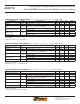
Power on Time versus External Filter Capacitance
0
20
40
60
80
100
120
140
160
180
200
0 10 20 30 40 50
C
F
(nF)
C
F
(nF)
t
PO
(µs)
I
P
=
5 A
I
P
=
0 A
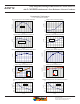
Noise versus External Filter Capacitance
1
1000
10
100
10000
0.01 0.1 1 10 100 1000
Noise
(p-p)
(mA)
Noise vs. Filter Cap
0.01 0.1 1 10
Filter Cap (nF)
ACS712
Noise vs. Filter Cap
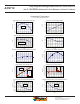
Rise Time versus External Filter Capacitance
1200
1000
800
600
400
200
0
0.1 1 10 100 1000
t
r
(µs)
C
F
(nF)
Rise Time versus External Filter Capacitance
180
160
140
120
100
80
60
40
20
0
0.1 1 10 100
t
r
(µs)
C
F
(nF)
Expanded in chart at right
}
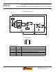
Definitions of Dynamic Response Characteristics
Primary Current
Transducer Output
90
10
0
I (%)
Rise Time, t
r
t
Rise time (t
r
). The time interval between a) when the device
reaches 10% of its full scale value, and b) when it reaches 90%
of its full scale value. The rise time to a step response is used to
derive the bandwidth of the device, in which ƒ(–3 dB) = 0.35 / t
r
.
Both t
r
and t
RESPONSE
are detrimentally affected by eddy current
losses observed in the conductive IC ground plane.
Excitation Signal
Output (mV)
15 A
Step Response
T
A
=25°C
C
F
(nF) t
r
(µs)
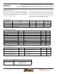
Open 3.5
1 5.8
4.7 17.5
22 73.5
47 88.2
100 291.3
220 623
470 1120
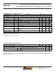
Power-On Time (t
PO
). When the supply is ramped to its operat-
ing voltage, the device requires a finite time to power its internal
components before responding to an input magnetic field.
Power-On Time, t
PO
, is defined as the time it takes for the output
voltage to settle within ±10% of its steady state value under an
applied magnetic field, after the power supply has reached its
minimum specified operating voltage, V
CC
(min), as shown in the
chart at right.