
Data Sheet


Fully Integrated, Hall Effect-Based Linear Current Sensor IC
with
2.1 kVRMS Isolation and a Low-Resistance Current Conductor
ACS712
9
Allegro MicroSystems, LLC
115 Northeast Cutoff
Worcester, Massachusetts 01615-0036 U.S.A.
1.508.853.5000; www.allegromicro.com
Sensitivity (Sens). The change in device output in response to a
1 A change through the primary conductor. The sensitivity is the
product of the magnetic circuit sensitivity (G / A) and the linear
IC amplifier gain (mV/G). The linear IC amplifier gain is pro-
grammed at the factory to optimize the sensitivity (mV/A) for the
full-scale current of the device.
Noise (V
NOISE
). The product of the linear IC amplifier gain
(mV/G) and the noise floor for the Allegro Hall effect linear IC
(≈1 G). The noise floor is derived from the thermal and shot
noise observed in Hall elements. Dividing the noise (mV) by the
sensitivity (mV/A) provides the smallest current that the device is
able to resolve.
Linearity (E
LIN
). The degree to which the voltage output from
the IC varies in direct proportion to the primary current through
its full-scale amplitude. Nonlinearity in the output can be attrib-
uted to the saturation of the flux concentrator approaching the
full-scale current. The following equation is used to derive the
linearity:
where V
IOUT_full-scale amperes
= the output voltage (V) when the
sampled current approximates full-scale ±I
P
.
Symmetry (E
SYM
). The degree to which the absolute voltage
output from the IC varies in proportion to either a positive or
negative full-scale primary current. The following formula is
used to derive symmetry:
Quiescent output voltage (V
IOUT(Q)
). The output of the device
when the primary current is zero. For a unipolar supply voltage,
it
nominally remains at V
CC
⁄ 2. Thus, V
CC
= 5 V translates into
V
IOUT(Q)
= 2.5 V. Variation in V
IOUT(Q)
can be attributed to the
resolution of the Allegro linear IC quiescent voltage trim and
thermal drift.
Electrical offset voltage (V
OE
). The deviation of the device out-
put from its ideal quiescent value of V
CC
/ 2 due to nonmagnetic
causes. To convert this voltage to amperes, divide by the device
sensitivity, Sens.
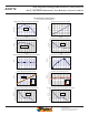
Accuracy (E
TOT
). The accuracy represents the maximum devia-
tion of the actual output from its ideal value. This is also known
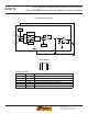
as the total output error. The accuracy is illustrated graphically in
the output voltage versus current chart at right.
Accuracy is divided into four areas:
• 0 A at 25°C. Accuracy at the zero current flow at 25°C, with-
out the effects of temperature.
• 0 A over Δ temperature. Accuracy at the zero current flow
including temperature effects.
• Full-scale current at 25°C. Accuracy at the the full-scale current
at 25°C, without the effects of temperature.
• Full-scale current over Δ temperature. Accuracy at the full-
scale current flow including temperature effects.
Ratiometry. The ratiometric feature means that its 0 A output,
V
IOUT(Q)
, (nominally equal to V
CC
/2) and sensitivity, Sens, are
proportional to its supply voltage, V
CC
. The following formula is
used to derive the ratiometric change in 0 A output voltage,
ΔV
IOUT(Q)RAT
(%).
The ratiometric change in sensitivity, ΔSens
RAT
(%), is defined as:
Definitions of Accuracy Characteristics
100
1–
[{
[{
V
IOUT_full-scale amperes
– V
IOUT(Q)
∆ gain × % sat (
)
2 (V
IOUT_half-scale amperes
– V
IOUT(Q)
)
100
V
IOUT_+ full-scale amperes
–
V
IOUT(Q)
V
IOUT(Q)
– V
IOUT_–full-scale amperes
100
V
IOUT(Q)VCC
/ V
IOUT(Q)5V
V
CC
/
5 V
100
Sens
VCC
/
Sens
5V
V
CC
/
5 V
‰
Output Voltage versus Sampled Current
Accuracy at 0 A and at Full-Scale Current
Increasing V
IOUT
(V)
+I
P
(A)
Accuracy
Accuracy
Accuracy
25°C Only
Accuracy
25°C Only
Accuracy
25°C Only
Accuracy
0 A
v rO e ∆Temp erature
Average
V
IOUT
–I
P
(A)
v rO e ∆Temp erature
v rO e ∆Temp erature
Decreasing V
IOUT
(V)
I
P
(min)
I
P
(max)
Full Scale