
Operating Manual


Additions
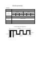
Picture7. DAC restrain RF interference circuit
1、RF antenna、TDD radiation noise
a)Picture7 is the circuit of DAC retrain RF antenna and TDD interference,itisrecommendedtoreserve,ifhas
limitedspacethencanjustreserveR6/R7/R8.
b)DAC、power supply lead and speaker cavity should avoid the RF position, the back of RF is the best position
for speaker and battery connection point.(Note: the noise disposing circuit of DAC will increase cost,if
solution design is reasonable enough and not highly require noise it can not be reserved.
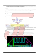
2
、
ESD disposing
Picture8. ESD static electricity disposing circuit
a) Likepicture8nearthechipDACVDD pin,AGND of C1 decoupling capacitor tandem connect capacitor
105 to GND nearby.
b) Likepicture8nearthechipRTCVDD pin ,RTCVDD tandem connect magnetic bead L1 ,thentandem
connect GNDof capacitor C3.(Note: ESD dispose will increase material, it can not be considered if solution
have no this requirement.)