
Operating Manual


Hardware Design Guidance
Power supply、ground wire
1、 Ground wire
The bluetooth ground wire are divided into AGND、PGND、and GND:
a)
AGND and GND must be strictly distinguished, connected at the battery entrance or in the front of IC
ground side; in the case of limited PCB board space, priority should be given to ensuring the connectivity of
GND and the battery ground circuit, and the route must be thick .
b) PGND and GND must be strictly distinguished,PGND go back to chip side behind of base pin and connect
GND nearby.
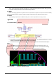
2、DCDC Picture 1. DC-DC switching power circuit
Like picture 1,
DC-DC
switching power circuit is composed of
SW
、
PGND
、BT_
AVDD、
L2、C3、C4、C9 (marked
red color);L2/C3/C4/C9 should be as close as possible to the base pin in layout;C3/C4/C9 ground circuit must return
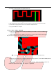
to the PGND pin at the shortest distance (no holes and as thick as possible), L2 + 1.5V routing must first pass the C4
(106) capacitort then go into IC (refer to picture 2);L2 should be as far away from the easily disturbed parts (such as
RF and DAC) as possible;. Do not install any signal line under the inductor or L2 should choose winding inductor or
power laminated inductor with minimum impedance
Picture 2. Ground Circuit of DC-DC Switching Power Supply