
Operating Manual


+1.5V power supply should as thick as possible and ,routing should first pass the capacitor then go into IC,it
is not allow to through the hole connect IC after passing capacitor .
3、LDOIN
LDOIN decoupling capacitor C5 is placed as close as possible to the pin of the chip and connected to PGND,
same time LDOIN should be as thick as possible, routing should first pass the capacitor then go into IC
4
、
VDDIO
The decoupling capacitor C6 of VDDIO should place as close as possible to the chip 2 pin side.
Signal line
1
、
Crystal oscillator Picture 3.
a) CrystaloscillatorY1shouldplaceascloseaspossibletothechippin,capacitorC23、C24 centralizedlayout(avoidC23、C24atthe
eachsideof crystaloscillator),andfindtheshortestwaytothechippin2(VSSIO);
b)IncaseofPCBsizeislimited,C24isallowedtobeplacednearthechipandmakesureitistheshortestdistancebacktochippin
2(VSSIO).
c)
CrystaloscillatorY1 requires good stability and consistency,frequency deviation within (±
10PPM);the size of loading capacitor C23 and C24 depend on the size of crystal oscillator loading
capacitor,be subjected to actual testing(recommend use JL matched crystal oscillator).
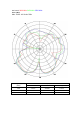
2
、
RF antenna Picture 4. Antenna layout