
Operating Manual


a)
RF
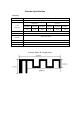
try place at the PCB side, can not have metal components on both front and back sides, use three -
side hollow-out way (top,left and right like picture 4).
Picture5.
b)RF and DAC circuit must in 180
0
layout to minimize the interference from RF to DAC .
c)If PCB have enough space be sure to use inverted F-shaped antenna.
d)Try to place RF like I -shaped.
3
、
DAC
、
MIC
、
VCOM
、
DACVDD
a)
DAC circuits and solder joints must be placed 180 degrees with RF to reduce the radiation and
interference from RF.
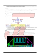
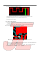
b) DAC circuits and solder joints ,AGND on the back or not, must not place under the DC-DC power
GND,otherwise there will be high- frequency noise, refer to picture 6.
Picture6. Wrong Layout and Routing of DAC Circuit Placed under DC-DC Power Circuit
c)MIC circuits and solder joints ,VCOM and DACVDD decoupling capacitors,withorwithout AGND,otherwise
easily beinterfered byRFandmake high frequency noise.
d) Do not lay “digital GND” under the three signal lines DACL、DACR and VCOMO ,as well as anti-
interference capacitors and inductors , stay away from “digitalGND”.