
User's Manual

SC14CVMDECT_SFxx_DB Reference Design
Antenna Productsheet
Date: August 15, 2013
Page 2 |
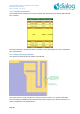
2.1.1 Design Parameters
The Printed Antenna Design has been developed and tested using the below depicted PCB
layer stackup:
The same PCB layer stackup should be used when using this design to ensure compliance
with specifications.
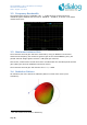
2.1.2 Physical Design Details
Here below the physical design details are depicted:
The visible grid is 0.5mm. Besides the antenna structure itself, it is critical to maintain
the exact same groundplane outline and spacing with respect to the antenna structure to
ensure compliance with specifications.