
User's Manual
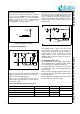
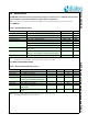


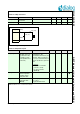


Table Of Contents
- 1.0 Connection diagram
- 2.0 Introduction
- 3.0 Specifications
- 3.1 GENERAL
- 3.2 ABSOLUTE MAXIMUM RATINGS
- 3.3 Operating Conditions
- 3.4 Digital Input/Output Pins
- 3.5 ULTRA LOW ENERGY (ULE) I/O PIN
- 3.6 SUPPLY CURRENTS
- 3.7 Analog Front End
- Table 10: Microphone amplifier
- Table 11: Microphone amplifier (Operating Condition)
- Table 12: Microphone supply voltages
- Table 13: VREFp load circuit
- Table 14: LSRp/LSRn outputs
- Table 15: LSRp/LSRn load circuits
- Table 16: PAOUTp, PAOUTn outputs
- Table 17: PAOUTp, PAOUTn outputs (Note 21)
- Table 18: PAOUTp, PAOUTn external components
- 3.8 Battery management
- 3.9 Baseband Part
- 3.10 Radio (RF) Part
- 3.11 RF Power supply
- 3.12 RF channel frequencies
- 4.0 Design guidelines
- 5.0 Notices to OEM
- 6.0 Package information
- 7.0 Revision history

SC14SPNODE SF DECT Module with integrated Antenna and FLASH
© 2012 Dialog Semiconductor B.V. 20 Jul 1, 2014 v1.6
3.10 RADIO (RF) PART
Standards compliancy: ETS 301 406 (former TBR6).
Table 22: Radio specifications
PARAMETER DESCRIPTION CONDITIONS MIN TYP MAX UNIT
P_Rx Receiver sensitivity BER = 0.001; TA = 25 °C -93 -92 -89 dBm
P_Rx_T Receiver sensitivity, full
temperature range
BER = 0.001;
-40 °C TA 85 °C
-94 -87 dBm
IPL Intermodulation perform-
ance level (EN 301 406
section 4.5.7.6)
TA = 25 °C;
Pw = -80 dBm;
f = 2 channels
-35 dBm
NTP Normal transmitted power DECT: 250 mW 24 26 dBm
J-DECT: 10 mW average per
frame for each slot
23 24.5 dBm
DECT6.0: 100 mW (max
peak)
20.0 dBm
dPrfpa_T RFPA power variation, full
temperature range
-40 °C TA +85 °C 2.5 4 dB
Fbit Bit rate GFSK modulation 1.152 Mbit/s
BW_Tx Transmitter bandwidth DECT GFSK;
NTP = 20 dB
1.728 MHz
Table 23: RFPA preferred settings for various power modes (PP application)
Address
(VES)
Register / Parameter
HPM/U
(USA)
HPM
(Europe)
HPM/J
(Japan)
0x3D RF_BBADC_CTRL_REG 0x0380 0x03A0 0x0398
0x39 RF_PA_CTRL1_REG 0x09A0 0x0CF0 0x2CE0
0x3B RF_TEST_MODE2_REG 0x0056 0x0062 0x0068
0x05 RF_PLL_CTRL2_REG[MODINDEX] 0x25 0x25 0x23
0x23 Upper RSSI threshold 0x2C N/A 0x28
0x24 Lower RSSI threshold 0x22 N/A 0x1E