
User's Manual


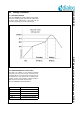


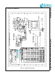
Table Of Contents
- 1.0 Connection diagram
- 2.0 Introduction
- 3.0 Specifications
- 3.1 GENERAL
- 3.2 ABSOLUTE MAXIMUM RATINGS
- 3.3 Operating Conditions
- 3.4 Digital Input/Output Pins
- 3.5 ULTRA LOW ENERGY (ULE) I/O PIN
- 3.6 SUPPLY CURRENTS
- 3.7 Analog Front End
- Table 10: Microphone amplifier
- Table 11: Microphone amplifier (Operating Condition)
- Table 12: Microphone supply voltages
- Table 13: VREFp load circuit
- Table 14: LSRp/LSRn outputs
- Table 15: LSRp/LSRn load circuits
- Table 16: PAOUTp, PAOUTn outputs
- Table 17: PAOUTp, PAOUTn outputs (Note 21)
- Table 18: PAOUTp, PAOUTn external components
- 3.8 Battery management
- 3.9 Baseband Part
- 3.10 Radio (RF) Part
- 3.11 RF Power supply
- 3.12 RF channel frequencies
- 4.0 Design guidelines
- 5.0 Notices to OEM
- 6.0 Package information
- 7.0 Revision history

SC14SPNODE SF DECT Module with integrated Antenna and FLASH
© 2012 Dialog Semiconductor B.V. 28 Jul 1, 2014 v1.6
6.3 COPPER PAD, SOLDER OPENING AND STEN-
CIL
For the stencil a thickness of 0.122 mm is
recommended. Recommended copper pad, solder
mask opening and stencil are shown below.
Figure 18 Pad dimensions