
User's Manual
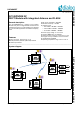
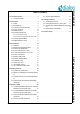
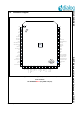
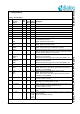
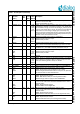

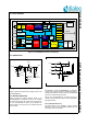
Table Of Contents
- 1.0 Connection diagram
- 2.0 Introduction
- 3.0 Specifications
- 3.1 GENERAL
- 3.2 ABSOLUTE MAXIMUM RATINGS
- 3.3 Operating Conditions
- 3.4 Digital Input/Output Pins
- 3.5 ULTRA LOW ENERGY (ULE) I/O PIN
- 3.6 SUPPLY CURRENTS
- 3.7 Analog Front End
- Table 10: Microphone amplifier
- Table 11: Microphone amplifier (Operating Condition)
- Table 12: Microphone supply voltages
- Table 13: VREFp load circuit
- Table 14: LSRp/LSRn outputs
- Table 15: LSRp/LSRn load circuits
- Table 16: PAOUTp, PAOUTn outputs
- Table 17: PAOUTp, PAOUTn outputs (Note 21)
- Table 18: PAOUTp, PAOUTn external components
- 3.8 Battery management
- 3.9 Baseband Part
- 3.10 Radio (RF) Part
- 3.11 RF Power supply
- 3.12 RF channel frequencies
- 4.0 Design guidelines
- 5.0 Notices to OEM
- 6.0 Package information
- 7.0 Revision history

SC14SPNODE SF DECT Module with integrated Antenna and FLASH
© 2012 Dialog Semiconductor B.V. 5 Jul 1, 2014 v1.6
22 CHARGE_CTRL O 1 O-0 ANALOG OUTPUT. Charge control pin. Supplied by internal VBAT
if device is off else from AVD.
Leave unconnected if not used.
23 CHARGE / P1[7] I - I-PD
(270k
fixed
pull-
down)
INPUT. Charger connected indication and supply voltage for power
management. Switches on the device if voltage > Vih_a3pad. Must
be connected to charger via resistor R>(Vcharger_max-3 V)/10 mA
(round to next largest value in range). An internal 10 ms hold circuit
keeps device on if the charger voltage ripple momentarily drop
below Vil_charge. This eliminates the use of expensive ripple filter.
If used as port pin, the maximum input switching speed of this pin is
100 kHz. Leave unconnected if not used.
24 PAOUTp
P3[1]
DP1
IO 500 O-0 (5k
fixed
pull-
down)
OUTPUT. CLASSD positive output to loudspeaker.
OUTPUT. General purpose output.
OUTPUT. DIP port DP1
25 VDDPA I - - CLASSD Audio Amplifier supply voltage up to 3.45 V.
GND or leave unconnected if PAOUT/P3[1:0] ports are not used.
26 CP_VOUT1 O - I Charge Pump Output 1.
A capacitor of 1 F to GND is internally connected to this pin.
27 PAOUTn
P3[0]
DP0
IO 500 O-0 (5k
fixed
pull-
down)
OUTPUT. CLASSD negative output to loudspeaker.
OUTPUT. General purpose output.
OUTPUT. DIP port DP0
28 GND - - - Ground
29 PON/
P1[6]
I-I (270k
fixed
pull-
down)
INPUT. Power on, Switches on the device if Voltage > Vih_a3pad.
May be directly connected to VBAT. If used as port pin, the maxi-
mum input switching speed of this pin is 100 kHz.
30 ULP_XTAL I - I 32.768 kHz XTAL clock input. Connect to GND if not used. (Note 7)
31 ULP_PORT I - I Ultra Low Power Port Pin. Connect to GND if not used. (Note 7)
32 P2[7]/
INT7
BXTAL
IO 8 I-PU INPUT/OUTPUT with selectable pull up/down resistor.
INPUT. Keyboard Interrupt.connected to P1[2] or P2[7].
OUTPUT. Digital buffered Xtal oscillator. This pin is not optimized
as reference clock for external RF devices.
33 P1[5]/
INT5/
RDI/
VDDE
IO 8 O-1 INPUT/OUTPUT with selectable pull up/down resistor.
INPUT. Keyboard input interrupt.
INPUT. BMC Receive data (for monitoring/external radio).
OUTPUT. P1[5] Used for supply of external EEPROM
34 P1[4]/
INT4/
TDOD
IO 1/2 I-PD INPUT/OUTPUT with selectable pull up/down resistor.
1 mA or 2 mA mode used to bias external NPN transistor without
external resistor.
INPUT. Keyboard input interrupt.
OUTPUT. BMC transmit digital data.
35 P1[3]/
INT3/
SIO
IO 1/2 I-PD INPUT/OUTPUT with selectable pull up/down resistor.
1 mA or 2 mA mode used to bias external NPN transistor without
external resistor.
INPUT. Keyboard input interrupt.
INPUT/OUTPUT. MicroWire data (for monitoring/external radio).
36 P1[2]/
INT2/
SK
IO 2 I-PD INPUT/OUTPUT with selectable pull up/down resistor.
INPUT. Keyboard input interrupt.
OUTPUT. MicroWire clock (for monitoring/external radio).
Table 1: Pin description (Continued)
Pin
Module
Pin name
(Note 1)
In/
Out
Iout
Drive
(mA)
Reset
State
(Note 2)
Description