
User's Manual
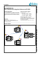
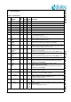
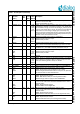

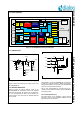
Table Of Contents
- 1.0 Connection diagram
- 2.0 Introduction
- 3.0 Specifications
- 3.1 GENERAL
- 3.2 ABSOLUTE MAXIMUM RATINGS
- 3.3 Operating Conditions
- 3.4 Digital Input/Output Pins
- 3.5 ULTRA LOW ENERGY (ULE) I/O PIN
- 3.6 SUPPLY CURRENTS
- 3.7 Analog Front End
- Table 10: Microphone amplifier
- Table 11: Microphone amplifier (Operating Condition)
- Table 12: Microphone supply voltages
- Table 13: VREFp load circuit
- Table 14: LSRp/LSRn outputs
- Table 15: LSRp/LSRn load circuits
- Table 16: PAOUTp, PAOUTn outputs
- Table 17: PAOUTp, PAOUTn outputs (Note 21)
- Table 18: PAOUTp, PAOUTn external components
- 3.8 Battery management
- 3.9 Baseband Part
- 3.10 Radio (RF) Part
- 3.11 RF Power supply
- 3.12 RF channel frequencies
- 4.0 Design guidelines
- 5.0 Notices to OEM
- 6.0 Package information
- 7.0 Revision history

SC14SPNODE SF DECT Module with integrated Antenna and FLASH
© 2012 Dialog Semiconductor B.V. 7 Jul 1, 2014 v1.6
56 P2[3]/
SDA1/
PCM_DI/
DP2
IO 8 I-PU INPUT/OUTPUT with selectable pull up/down resistor.
INPUT / OUTPUT. ACCESS bus 1 data with programmable Push-
pull or open drain.
INPUT. PCM data input.
OUTPUT. DIP port DP2.
57 P2[2]/
PCM_CLK/
CLK100
I/O 8 I-PD INPUT/OUTPUT with selectable pull up/down resistor.
INPUT/OUTPUT. PCM clock.
OUTPUT. DIP 100 Hz output.
58 P2[1]/
ECZ2/
PWM1/
LED4
IO 8 I INPUT/OUTPUT with selectable pull up/down resistor.
OUTPUT. Gen2DSP output port.
OUTPUT. Timer 0 PWM 1 output.
LED4: 2.5 mA/5 mA LED current sink.
59 P2[0]/
ECZ1/
PWM0/
LED3
IO 8 I INPUT/OUTPUT with selectable pull up/down resistor.
OUTPUT. Gen2DSP output port.
OUTPUT. Timer 0 PWM 0 output.
LED3: 2.5 mA/5 mA LED current sink.
60 GND - - - Ground
61 VDDOUT - - - Test purpose only. Must be left unconnected. See 2.5
62 VBATSW Test purpose only. Must be left unconnected. See 2.5
63 VBATIN I - - Main supply voltage < 3.45 V. See 2.5
64 VBATIN I - - Main supply voltage < 3.45 V. See 2.5
65 P3[2]/
CIDINp/
IO 8 I INPUT/OUTPUT with selectable pull up/down resistor.
INPUT. Caller-id opamp positive input with switchable input protec-
tion enabled from start-up.
66 P3[7]/
RINGp
IO 4 I INPUT/OUTPUT with selectable pull up/down resistor.
ANALOG INPUT. Positive ringing signal opamp input with switcha-
ble input protection.
67 P3[6] /
RINGn
IO 4 I INPUT/OUTPUT with selectable pull up/down resistor.
ANALOG INPUT. Negative ringing signal opamp input with switcha-
ble input protection.
68 P3[5]/
RINGOUT/
RINGING
IO 4 I INPUT/OUTPUT with selectable pull up/down resistor.
OUTPUT. Ringing opamp output to ADC.
INPUT. Ringer signal detection input to capture timers and ADC.
69 P3[4]/
PARADET
IO 8 I INPUT/OUTPUT with selectable pull up/down resistor.
ANALOG INPUT. Parallel set detection input to ADC with switcha-
ble input protection.
70 GND - - - Ground
71 GND - - - Ground
72 GND - - - Ground
73 RF1 - - - RF signal for external antenna. See 2.6
74 GND - - - Ground
75 RF0 - - - RF signal for external antenna. See 2.6
76 GND - - - Ground
77 GND - - - Ground
78 GND - - - Ground
79 TP1 - - - Tuning point for internal antenna. Follow instructions of section 4.3.
80 GND - - - Ground
Table 1: Pin description (Continued)
Pin
Module
Pin name
(Note 1)
In/
Out
Iout
Drive
(mA)
Reset
State
(Note 2)
Description