
User Manual
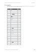

PCB design and manufacturing Recommended footprint and keepout
XBee/XBee-PRO S2C 802.15.4 RF Module User Guide
148
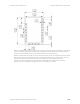
Match the solder footprint to the copper pads, but you may need to adjust it depending on the specific
needs of assembly and product standards. We recommend a stencil thickness of 0.15 mm (0.005 in).
Place the component last and set the placement speed to the slowest setting.
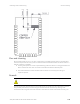
While the underside of the module is mostly coated with solder resist, we recommend that the copper
layer directly below the module be left open to avoid unintended contacts. Copper or vias must not
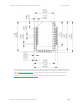
interfere with the three exposed RF test points on the bottom of the module (see below).
Furthermore, these modules have a ground plane in the middle on the back side for shielding
purposes, which can be affected by copper traces directly below the module.