Spartan-3 Starter Kit Board User Guide UG130 (v1.
R "Xilinx" and the Xilinx logo shown above are registered trademarks of Xilinx, Inc. Any rights not expressly granted herein are reserved. CoolRunner, RocketChips, Rocket IP, Spartan, StateBENCH, StateCAD, Virtex, XACT, XC2064, XC3090, XC4005, and XC5210 are registered trademarks of Xilinx, Inc. The shadow X shown above is a trademark of Xilinx, Inc. ACE Controller, ACE Flash, A.K.A.
Table of Contents Preface: About This Guide Guide Contents . . . . . . . . . . . . . . . . . . . . . . . . . . . . . . . . . . . . . . . . . . . . . . . . . . . . . . . . . . . . . . 5 Chapter 1: Introduction Key Components and Features . . . . . . . . . . . . . . . . . . . . . . . . . . . . . . . . . . . . . . . . . . . . . . . 7 Component Locations . . . . . . . . . . . . . . . . . . . . . . . . . . . . . . . . . . . . . . . . . . . . . . . . . . . . . . . .
R Chapter 10: Platform Flash Configuration Storage Platform Flash Jumper Options (JP1) . . . . . . . . . . . . . . . . . . . . . . . . . . . . . . . . . . . . . . . . “Default” Option . . . . . . . . . . . . . . . . . . . . . . . . . . . . . . . . . . . . . . . . . . . . . . . . . . . . . . . . . . . “Flash Read” Option . . . . . . . . . . . . . . . . . . . . . . . . . . . . . . . . . . . . . . . . . . . . . . . . . . . . . . . . “Disable” Option . . . . . . . . . . . . . . . . . . . . . . . . . . . . . .
R Preface About This Guide This user guide describes the components and operation of the Spartan™-3 Starter Kit Board.
R 6 Preface: About This Guide www.xilinx.com 1-800-255-7778 Spartan-3 Starter Kit Board User Guide UG130 (v1.
R Chapter 1 Introduction The Xilinx Spartan-3 Starter Kit provides a low-cost, easy-to-use development and evaluation platform for Spartan-3 FPGA designs.
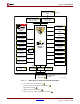
R Chapter 1: Introduction Digilent Low-Cost 23 Parallel Port to JTAG Included Cable Parallel Cable IV 24 MutliPro Desktop Tool JTAG Connector Low-Cost JTAG Download Cable Connector 22 A1 Expansion Header 21 XCF02S 2Mbit Configuration PROM A2 Expansion Header 20 Platform Flash Option Jumpers B1 Expansion Header 19 256Kx16 10ns SRAM Configuration DONE LED 18 PROGRAM Push Button 17 Configuration Mode Select Jumpers 16 2 3 4 1 256Kx16 10ns SRAM 5 8-color VGA Port 6 RS-232 Port Serial
R Component Locations • 50 MHz crystal oscillator clock source (bottom side of board, see Figure 1-3) • Socket for an auxiliary crystal oscillator clock source • FPGA configuration mode selected via jumper settings • Push button switch to force FPGA reconfiguration (FPGA configuration happens automatically at power-on) 17 • LED indicates when FPGA is successfully configured • Three 40-pin expansion connection ports to extend and enhance the Spartan-3 Starter Kit Board 19 20 21 14 15 16 18 ♦
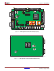
R Chapter 1: Introduction 21 20 A1 Expansion Connector A2 Expansion Connector 31 2 27 24 VGA 16 17 3 XILINX XC3S200 FPGA 18 DONE 25 19 2Mbit PlatformFlash B1 Expansion Connector 3.3V 22 5 PROG 1 POWER POWER 26 RS-232 RS-232 6 7 15 10 12 30 8 PS/2 9 11 13 ug130_c1_02_042704 Figure 1-2: Xilinx Spartan-3 Starter Kit Board (Top Side) 5 256Kx16 SRAM 256Kx16 SRAM 4 2.5V 28 29 50 MHz 1.
R Chapter 2 Fast, Asynchronous SRAM The Spartan-3 Starter Kit board has a megabyte of fast asynchronous SRAM, surfacemounted to the backside of the board. The memory array includes two 256Kx16 ISSI IS61LV25616AL-10T 10 ns SRAM devices, as shown in Figure 2-1. A detailed schematic appears in Figure A-8.
R Chapter 2: Fast, Asynchronous SRAM The SRAM array forms either a single 256Kx32 SRAM memory or two independent 256Kx16 arrays. Both SRAM devices share common write-enable (WE#), output-enable (OE#), and address (A[17:0]) signals. However, each device has a separate chip select enable (CE#) control and individual byte-enable controls to select the high or low byte in the 16-bit data word, UB and LB, respectively. The 256Kx32 configuration is ideally suited to hold MicroBlaze instructions.
R Write Enable and Output Enable Control Signals Write Enable and Output Enable Control Signals Both 256Kx16 SRAMs share common output enable (OE#) and write enable (WE#) control lines, as shown in Table 2-2. These control signals also connect to the A1 Expansion Connector (refer to “Expansion Connectors,” page 47).
R Chapter 2: Fast, Asynchronous SRAM Table 2-4: SRAM IC11 Connections 14 Signal FPGA Pin IO15 N1 IO14 M1 IO13 K2 IO12 C3 IO11 F5 IO10 G1 IO9 E2 IO8 D2 IO7 D1 IO6 E1 IO5 G2 IO4 J1 IO3 K1 IO2 M2 IO1 N2 IO0 P2 CE2 (chip enable IC11) N5 UB2 (upper byte enable IC11) R4 LB2 (lower byte enable IC11) P5 www.xilinx.com 1-800-255-7778 Spartan-3 Starter Kit Board User Guide UG130 (v1.
R Chapter 3 Four-Digit, Seven-Segment LED Display The Spartan-3 Starter Kit board has a four-character, seven segment LED display controlled by FPGA user-I/O pins, as shown in Figure 3-1. Each digit shares eight common control signals to light individual LED segments. Each individual character has a separate anode control input. A detailed schematic for the display appears in Figure A-2. The pin number for each FPGA pin connected to the LED display appears in parentheses.
R Chapter 3: Four-Digit, Seven-Segment LED Display Table 3-1: FPGA Connections to Seven-Segment Display (Active Low) Segment FPGA Pin A E14 B G13 C N15 D P15 E R16 F F13 G N16 DP P16 Table 3-2: Digit Enable (Anode Control) Signals (Active Low) Anode Control AN3 AN2 AN1 AN0 FPGA Pin E13 F14 G14 D14 Table 3-3: Display Characters and Resulting LED Segment Control Values 16 Character a b c d e f g 0 0 0 0 0 0 0 1 1 1 0 0 1 1 1 1 2 0 0 1 0 0 1 0 3
R The LED control signals are time-multiplexed to display data on all four characters, as shown in Figure 3-2. Present the value to be displayed on the segment control inputs and select the specified character by driving the associated anode control signal Low. Through persistence of vision, the human brain perceives that all four characters appear simultaneously, similar to the way the brain perceives a TV display.
R 18 Chapter 3: Four-Digit, Seven-Segment LED Display www.xilinx.com 1-800-255-7778 Spartan-3 Starter Kit Board User Guide UG130 (v1.
R Chapter 4 Switches and LEDs Slide Switches The Spartan-3 Starter Kit board has eight slide switches, indicated as 11 in Figure 1-2. The switches are located along the lower edge of the board, toward the right edge. The switches are labeled SW7 through SW0. Switch SW7 is the left-most switch, and SW0 is the rightmost switch. The switches connect to an associated FPGA pin, as shown in Table 4-1. A detailed schematic appears in Figure A-2.
R Chapter 4: Switches and LEDs LEDs The Spartan-3 Starter Kit board has eight individual surface-mount LEDs located above the push button switches, indicated by 12 in Figure 1-2. The LEDs are labeled LED7 through LED0. LED7 is the left-most LED, LED0 the right-most LED. Table 4-3 shows the FPGA connections to the LEDs.
R Chapter 5 VGA Port The Spartan-3 Starter Kit board includes a VGA display port and DB15 connector, indicated as 5 in Figure 1-2. Connect this port directly to most PC monitors or flat-panel LCD displays using a standard monitor cable.
R Chapter 5: VGA Port Table 5-1: VGA Port Connections to the Spartan-3 FPGA Signal FPGA Pin Red (R) R12 Green (G) T12 Blue (B) R11 Horizontal Sync (HS) R9 Vertical Sync (VS) T10 Each color line has a series resistor to provide 3-bit color, with one bit each for Red, Green, and Blue. The series resistor uses the 75Ω VGA cable termination to ensure that the color signals remain in the VGA-specified 0V to 0.7V range. The HS and VS signals are TTL level.
R Signal Timing for a 60Hz, 640x480 VGA Display same signal timings as CRT displays. Consequently, the following discussion pertains to both CRTs and LCD displays. Within a CRT display, current waveforms pass through the coils to produce magnetic fields that deflect electron beams to transverse the display surface in a “raster” pattern, horizontally from left to right and vertically from top to bottom.
R Chapter 5: VGA Port Modern VGA displays support multiple display resolutions, and the VGA controller dictates the resolution by producing timing signals to control the raster patterns. The controller produces TTL-level synchronizing pulses that set the frequency at which current flows through the deflection coils, and it ensures that pixel or video data is applied to the electron guns at the correct time.
R VGA Signal Timing Generally, a counter clocked by the pixel clock controls the horizontal timing. Decoded counter values generate the HS signal. This counter tracks the current pixel display location on a given row. A separate counter tracks the vertical timing. The vertical-sync counter increments with each HS pulse and decoded values generate the VS signal. This counter tracks the current display row. These two continuously running counters form the address into a video display buffer.
R 26 Chapter 5: VGA Port www.xilinx.com 1-800-255-7778 Spartan-3 Starter Kit Board User Guide UG130 (v1.
R Chapter 6 PS/2 Mouse/Keyboard Port The Spartan-3 Starter Kit board includes a PS/2 mouse/keyboard port and the standard 6pin mini-DIN connector, labeled J3 on the board and indicated as 9 in Figure 1-2. Figure 6-1 shows the PS/2 connector, and Table 6-1 shows the signals on the connector. Only pins 1 and 5 of the connector attach to the FPGA. A detailed schematic appears in Figure A-7.
R Chapter 6: PS/2 Mouse/Keyboard Port bidirectional keyboard communications. As shown in Figure 6-2, the attached keyboard or mouse writes a bit on the data line when the clock signal is High, and the host reads the data line when the clock signal is Low.
R Keyboard ESC 76 `~ 0E 1! 16 TAB 0D Caps Lock 58 Shift 12 F1 05 F2 06 2@ 1E 3# 26 Q 15 W 1D A 1C F4 0C 4$ 25 E 24 S 1B Z 1Z Ctrl 14 F3 04 5% 2E R 2D D 23 X 22 F5 03 6^ 36 T 2C F 2B C 21 F6 0B 7& 3D Y 35 G 34 V 2A F8 0A 8* 3E U 3C H 33 B 32 Alt 11 F7 83 9( 46 I 43 J 3B N 31 F10 09 -_ 4E =+ 55 0) 45 O 44 K 42 M 3A F9 01 P 4D L 4B ,< 41 Space 29 [{ 54 ;: 4C >.
R Chapter 6: PS/2 Mouse/Keyboard Port The following site contains more information on PS/2 keyboard interfaces: • The AT-PS/2 Keyboard Interface http://panda.cs.ndsu.nodak.edu/~achapwes/PICmicro/keyboard/atkeyboard.html Mouse A mouse generates a clock and data signal when moved; otherwise, these signals remain High indicating the Idle state. Each time the mouse is moved, the mouse sends three 11-bit words to the host.
R Voltage Supply when an overflow occurs. If the mouse moves continuously, the 33-bit transmissions repeat every 50 ms or so. The L and R fields in the status byte indicate Left and Right button presses. A ‘1’ indicates that the associated mouse button is being pressed. The following site contains additional information on interfacing to a PS/2-style mouse: • The PS/2 Mouse Interface http://panda.cs.ndsu.nodak.edu/~achapwes/PICmicro/mouse/mouse.
R 32 Chapter 6: PS/2 Mouse/Keyboard Port www.xilinx.com 1-800-255-7778 Spartan-3 Starter Kit Board User Guide UG130 (v1.
R Chapter 7 RS-232 Serial Port The Spartan-3 Starter Kit board has an RS-232 serial port. The RS-232 transmit and receive signals appear on the female DB9 connector, labeled J2, indicated as 6 in Figure 1-2. The connector is a DCE-style port and connects to the DB9 DTE-style serial port connector available on most personal computers and workstations. Use a standard straight-through serial cable to connect the Spartan-3 Starter Kit board to the PC’s serial port.
R Chapter 7: RS-232 Serial Port device converts the RS-232 serial input data to LVTLL levels for the FPGA. A series resistor between the Maxim output pin and the FPGA’s RXD pin protects against accidental logic conflicts. A detailed schematic appears in Figure A-7. Hardware flow control is not supported on the connector. The port’s DCD, DTR, and DSR signals connect together, as shown in Figure 7-1. Similarly, the port’s RTS and CTS signals connect together.
R Chapter 8 Clock Sources The Spartan-3 Starter Kit board has a dedicated 50 MHz Epson SG-8002JF series clock oscillator source and an optional socket for another clock oscillator source. Figure A-5 provides a detailed schematic for the clock sources. The 50 MHz clock oscillator is mounted on the bottom side of the board, indicated as 14 in Figure A-5. Use the 50 MHz clock frequency as is or derive other frequencies using the FPGAs Digital Clock Managers (DCMs).
R Chapter 9: FPGA Configuration Modes and Functions Chapter 9 FPGA Configuration Modes and Functions FPGA Configuration Mode Settings In most applications for the Spartan-3 Starter Kit Board, the FPGA automatically boots from the on-board Platform Flash memory whenever power is applied or the PROG push button is pressed. However, the board supports all the available configuration modes via the J8 header, indicated as 16 in Figure 1-2. Table 9-1 provides the available option settings for the J8 header.
R Program Push Button/DONE Indicator LED Table 9-1: Header J8 Controls the FPGA Configuration Mode (Continued) Slave Parallel Header J8 Settings Jumper JP1 Setting GND J8 JP1 Another device connected to the B1 expansion connector provides parallel data and clock to load the FPGA. JP1 The FPGA waits for configuration via the four-wire JTAG interface.
R Chapter 10 Platform Flash Configuration Storage The Spartan-3 Starter Kit board has an XCF02S serial configuration Flash PROM to store FPGA configuration data and potentially additional non-volatile data, including MicroBlaze application code. To configure the FPGA from Platform Flash memory, all three jumpers must be installed on the J8 header, indicated as 16 in Figure 1-2.
R “Flash Read” Option Spartan-3 FPGA Platform Flash JP1 M0 DIN/D0 D0 M1 INIT_B OE/RESET M2 DONE CE CCLK CLK Default MODE J8 USER I/O RCLK UG130_c10_01_060704 Figure 10-1: Default Platform Flash Option “Flash Read” Option The Spartan-3 Starter Kit Board includes a 2Mbit Platform Flash configuration PROM. The XC3S200 FPGA on the board only requires slightly less than 1Mbit for configuration data.
R Chapter 10: Platform Flash Configuration Storage Additional FPGA logic is required to read the Platform Flash data, as described in the following application note. • XAPP694: Reading User Data from Configuration PROMs http://www.xilinx.com/bvdocs/appnotes/xapp694.pdf “Disable” Option If the JP1 jumper is removed, then the Platform Flash is disabled, potentially allowing configuration via an expansion board connected to one of the expansion connectors. 40 www.xilinx.
R Chapter 11 JTAG Programming/Debugging Ports The Spartan-3 Starter Kit board includes a JTAG programming and debugging chain. Both the Spartan-3 FPGA and the Platform Flash devices are part of the JTAG chain, as shown in Figure 11-1. Additionally, there are two JTAG headers for driving the JTAG signals from various supported JTAG download and debugging cables. A Digilent JTAG3 low-cost parallel to JTAG cable is included as part of the kit and connects to the J7 header.
R Chapter 11: JTAG Programming/Debugging Ports TMS TDI TDO 2.8V TCK GND UP TO 5V VCC 23 21 J7 TMS TDI TDO TCK GND VDD 20 22 UG130_c11_02_042704 Figure 11-2: Digilent JTAG Cable Provided with Kit Connects to the J7 Header The J7 header also supports the Xilinx Parallel Cable 3 (PC3) download/debugging cable when using the flying leaders. Again, make sure that the signals at the end of the JTAG cable align with the labels listed on the board.
R Parallel Cable IV/MultiPro Desktop Tool JTAG Header (J5) Red trace indicates pin 1 21 20 24 J5 Parallel Cable IV JTAG Notch on outline matches key on header UG130_c11_03_042704 Figure 11-3: Use 14-Pin Ribbon Cable to Connect Parallel Cable IV or the MultiPro Desktop Tool to the J5 Header Spartan-3 Starter Kit Board User Guide UG130 (v1.1) May 13, 2005 www.xilinx.
R 44 Chapter 11: JTAG Programming/Debugging Ports www.xilinx.com 1-800-255-7778 Spartan-3 Starter Kit Board User Guide UG130 (v1.
R Chapter 12 Power Distribution AC Wall Adapter The Spartan-3 Starter Kit includes an international-ready AC wall adapter that produces a +5V DC output. Connect the AC wall adapter to the barrel connector along the left edge of the board, indicated as 25 in Figure 1-2. There is no power switch to the board. To disconnect power, remove the AC adapter from the wall or disconnect the barrel connector. The POWER indicator LED, shown as 26 in Figure 1-2, lights up when power is properly applied to the board.
R Chapter 12: Power Distribution 2.5V and 1.2V regulators. Similarly, the 3.3V regulator feeds all the VCCO voltage supply inputs to the FPGA’s I/O banks and powers most of the components on the board. The 2.5V regulator supplies power to the FPGA’s VCCAUX supply inputs. The VCCAUX voltage input supplies power to Digital Clock Managers (DCMs) within the FPGA and supplies some of the I/O structures.
R Chapter 13 Expansion Connectors and Boards Expansion Connectors The Spartan-3 Starter Kit board has three 40-pin expansion connectors labeled A1, A2, and B1. The A1 and A2 connectors, indicated as 21 and 20 , respectively, in Figure 1-2, are on the top edge of the board. Connector A1 is on the top left, and A2 is on the top right. The B1 connector, indicated as 19 in Figure 1-2, is along the right edge of the board.
R Chapter 13: Expansion Connectors and Boards Table 13-1: Expansion Connector Features Connector User I/O SRAM JTAG Serial Configuration A1 32 Address OE#, WE# Data[7:0] to IC10 only √ A2 34 √ B1 34 √ Parallel Configuration √ Each port offers some ability to program the FPGA on the Spartan-3 Starter Kit Board. For example, port A1 provides additional logic to drive the FPGA and Platform Flash JTAG chain.
R Expansion Connectors A1 Connector Pinout The A1 expansion connector is located along the top edge of the board, on the left, as indicated by 21 in Figure 1-2. Table 13-2 provides the pinout for the A1 connector. The FPGA connections are specified in parentheses. Table 13-2: Pinout for A1 Expansion Connector Schematic Name FPGA Pin GND Connector 1 2 FPGA Pin Schematic Name VU (+5V) VCCO (+3.
R Chapter 13: Expansion Connectors and Boards The A1 expansion connector shares connections with the 256Kx16 SRAM devices, specifically the SRAM address lines, the OE# and WE# control signals, and the eight leastsignificant data lines to SRAM IC10 only. Similarly, the JTAG chain is available on pins 36 through 40. Pin 20 is the FPGA DOUT/BUSY configuration signal and toggles during the FPGA configuration process.
R Expansion Connectors B1 Connector Pinout The B1 expansion connector is located on the right edge of the board, as indicated by 19 in Figure 1-2. Table 13-4 provides the pinout for the B1 connector. The FPGA connections are specified in parentheses. Most of the B1 expansion connector pins connect only with the FPGA and are not shared. Pins 36 through 40 include the signals required to configure the FPGA in Master or Slave Serial mode.
R Chapter 13: Expansion Connectors and Boards Expansion Boards Various expansion boards plug into the A1, A2, or B1 connectors as listed below: 52 • Spartan-3 Starter Kit Expansion Boards http://www.xilinx.com/s3boards • Digilent Expansion Boards https://digilent.us/Sales/boards.cfm#Peripheral • Digilent Breakout Probe Header (TPH1) https://digilent.us/Sales/Product.cfm?Prod=TPH1 • Digilent Breadboard (DBB1) https://digilent.us/Sales/Product.
R Appendix A Board Schematics This appendix provides the schematics for the Spartan-3 Starter Kit Board: • Figure A-1, “A1, A2, and B1 Expansion Connectors” • Figure A-2, “Slide Switches, Push Buttons, LEDs, and Four-Character 7-Segment Display” • Figure A-3, “Voltage Regulators, JP2 Jumper Setting for PS/2 Port Voltage” • Figure A-4, “FPGA Configuration Interface, Platform Flash, JTAG Connections, Jumper JP1” • Figure A-5, “FPGA I/O Connections, Clock Sources” • Figure A-6, “Power Decoupling C
R Appendix A: Board Schematics UG130_ApA_01_051305 Spartan-3 Starter Kit Board User Guide UG130 (v1.1) May 13, 2005 Figure A-1: A1, A2, and B1 Expansion Connectors www.xilinx.com 1-800-255-7778 NOTE: SRAM address lines and OE#, WE# controls have shared connections with A1 connector. Likewise, lower eight data bits to SRAM IC10 are also shared with A1 connector.
www.xilinx.com 1-800-255-7778 UG130_ApA_02_051305 Figure A-2: Slide Switches, Push Buttons, LEDs, and Four-Character 7-Segment Display Spartan-3 Starter Kit Board User Guide UG130 (v1.
R Appendix A: Board Schematics UG130_ApA_03_042704 Spartan-3 Starter Kit Board User Guide UG130 (v1.1) May 13, 2005 Figure A-3: Voltage Regulators, JP2 Jumper Setting for PS/2 Port Voltage www.xilinx.
www.xilinx.com 1-800-255-7778 UG130_ApA_04_051305 Figure A-4: FPGA Configuration Interface, Platform Flash, JTAG Connections, Jumper JP1 Spartan-3 Starter Kit Board User Guide UG130 (v1.
R Appendix A: Board Schematics UG130_ApA_05_051305 Spartan-3 Starter Kit Board User Guide UG130 (v1.1) May 13, 2005 Figure A-5: FPGA I/O Connections, Clock Sources www.xilinx.
www.xilinx.com 1-800-255-7778 Figure A-6: Power Decoupling Capacitors Spartan-3 Starter Kit Board User Guide UG130 (v1.
R Appendix A: Board Schematics UG130_ApA_07_051305 Spartan-3 Starter Kit Board User Guide UG130 (v1.1) May 13, 2005 Figure A-7: RS-232 Serial Port, VGA Port, PS/2 Port, Parallel Cable IV JTAG Interface www.xilinx.
Figure A-8: Spartan-3 Starter Kit Board User Guide UG130 (v1.1) May 13, 2005 2x256Kx16 Fast Asynchronous SRAM Interface www.xilinx.com 1-800-255-7778 NOTE: SRAM address lines and OE#, WE# controls have shared connections with A1 connector. Likewise, lower eight data bits to SRAM IC10 are also shared with A1 connector.
R Appendix A: Board Schematics UG130_ApA_09_042604 Spartan-3 Starter Kit Board User Guide UG130 (v1.1) May 13, 2005 Figure A-9: Digilent JTAG3 Low-Cost JTAG Download/Debug Cable www.xilinx.
R Appendix B Reference Material for Major Components Table B-1 lists the major components on the Spartan-3 Starter Kit Board, including full part numbers and links to complete device data sheets. Table B-1: Major Components and Data Sheet Links Device 1 Vendor Part Number Xilinx, Inc. XC3S200-4FT256C Spartan-3 FPGA http://www.xilinx.com/bvdocs/publications/ds099.pdf Xilinx, Inc. XCF02SVO20C Platform Flash Configuration Flash PROM http://www.xilinx.com/bvdocs/publications/ds123.
R www.xilinx.com/s3boards PN 0402292 www.xilinx.com 1-800-255-7778 Spartan-3 Starter Kit Board User Guide UG130 (v1.