
Manual

34 www.xilinx.com Spartan-3 Starter Kit Board User Guide
1-800-255-7778 UG130 (v1.1) May 13, 2005
Chapter 7:
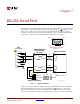
RS-232 Serial Port
R
device converts the RS-232 serial input data to LVTLL levels for the FPGA. A series resistor
between the Maxim output pin and the FPGA’s RXD pin protects against accidental logic
conflicts. A detailed schematic appears in Figure A-7.
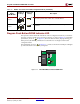
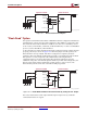
Hardware flow control is not supported on the connector. The port’s DCD, DTR, and DSR
signals connect together, as shown in Figure 7-1. Similarly, the port’s RTS and CTS signals
connect together.
The FPGA connections to the Maxim RS-232 translator appear in Table 7-1.
An auxiliary RS-232 serial channel from the Maxim device is available on two 0.1-inch
stake pins, indicated as J1 in the schematic and in Figure 1-2. The J1 stake pins are in
the lower left corner of the board, to the right of the DB9 serial connector, below the Maxim
RS-232 voltage translator, and to the left of the individual LEDs. The transmitter output
from the Maxim device drives the bottom stake pin while the receiver input connects to the
top stake pin.
The FPGA auxiliary RS-232 connections to the Maxim device appear in Table 7-1 with
signals RXD-A and TXD-A. Ignore the pin numbers listed on the silkscreen markings next
to the stake pins as these apply to the connections to the DB9 connector.
Place a jumper across the stake pins for an easy loop-back test. Alternately, create custom
serial ports by attaching the stake pins to other types of serial connectors such as male or
female DB9 or DB25 cable connectors or even create null modem connections.
Table 7-1:
Accessory Port Connections to the Spartan-3 FPGA
Signal FPGA Pin
RXD T13
TXD R13
RXD-A N10
TXD-A T14
8